TSMC introduced its next-generation A14 logic process at the North America Technology Symposium in Santa Clara, California, outlining a significant performance and power advancement over its forthcoming N2 node. Slated for production in 2028, A14 promises up to 15% speed gains or 30% power reduction, along with a 20% increase in logic density. The process builds on TSMC’s experience with nanosheet transistor architectures and introduces a new NanoFlex™ Pro standard cell architecture for greater design flexibility.
A14 headlines TSMC’s expanding portfolio targeting AI, HPC, smartphone, automotive, and IoT applications. In HPC, TSMC will bring a 9.5-reticle CoWoS® platform to volume in 2027 to support up to 12 HBM stacks. The company also unveiled SoW-X, a wafer-scale integration platform offering 40x the compute of current CoWoS configurations. For edge AI, TSMC announced N4C RF for WiFi8 and AI-rich audio, and reaffirmed automotive-grade readiness for N3A targeting ADAS and autonomous driving. In IoT, N4e will continue TSMC’s push for ultra-low-power edge AI.
TSMC also highlighted advancements in silicon photonics (COUPE), integrated voltage regulation (IVR) for AI workloads, and foundational support for 3D chip stacking. The event drew over 2,500 attendees and featured an Innovation Zone showcasing early-stage companies developing next-generation compute, connectivity, and semiconductor solutions.
- A14 logic process enters production in 2028 with 15% speed or 30% power gains over N2.
- NanoFlex Pro architecture introduced for enhanced performance and design flexibility.
- 9.5-reticle CoWoS and wafer-scale SoW-X platforms target AI and HBM integration.
- N4C RF enables WiFi8 and AI audio for edge devices; N3A reaches automotive-grade readiness.
- TSMC’s N4e and N6e extend ultra-low power capabilities to edge IoT AI applications.
“TSMC’s cutting-edge logic technologies like A14 are part of a comprehensive suite of solutions that connect the physical and digital worlds to unleash our customers’ innovation for advancing the AI future,” said Dr. C.C. Wei, Chairman and CEO of TSMC.
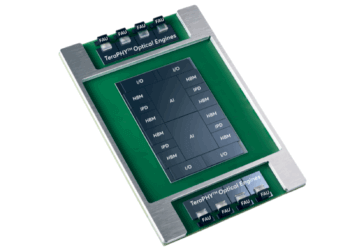
About COUPE
TSMC’s Compact Universal Photonic Engine (COUPE) represents a significant advancement in silicon photonics, aiming to address the growing demands for high-bandwidth, low-power interconnects in data-intensive applications such as AI, high-performance computing (HPC), and data centers.
COUPE is a silicon photonics integration platform that combines electronic integrated circuits (EICs) with photonic integrated circuits (PICs) using TSMC’s advanced packaging technologies. This integration facilitates efficient optical communication within and between chips, offering substantial improvements in data transfer rates and energy efficiency.
Key Features and Benefits
- High Bandwidth and Energy Efficiency: COUPE enables data transfer rates up to 12.8 Tbps while significantly reducing power consumption compared to traditional electrical interconnects .
- Advanced Packaging: Utilizing TSMC’s SoIC-X (System on Integrated Chips) technology, COUPE achieves low-impedance connections between EICs and PICs, enhancing signal integrity and performance .
- Scalability: The modular design of COUPE allows for integration into various system architectures, supporting applications ranging from data centers to edge computing devices.
Development Roadmap
TSMC’s COUPE development is structured in multiple phases:
- First Generation: Targeting 1.6 Tbps data rates, suitable for OSFP (Octal Small Form Factor Pluggable) modules, with mass production anticipated in the second half of 2026 .
- Second Generation: Aiming for 6.4 Tbps, integrating COUPE into CoWoS (Chip on Wafer on Substrate) packaging for co-packaged optics with switches.
- Third Generation: Projected to achieve 12.8 Tbps, focusing on full integration into processor packages, currently in the exploratory phase .
TSMC collaborates with industry leaders like Ansys and Synopsys to enhance COUPE’s capabilities:
- Ansys: Provides multiphysics simulation tools for optical, thermal, and electromagnetic analysis, ensuring reliable COUPE designs .
- Synopsys: Offers design automation solutions for photonic integrated circuits, streamlining the development process .