Multibeam Corp. raised $31 million in an oversubscribed Series B round to accelerate development of its multi-column electron beam lithography (EBL) systems for advanced semiconductor applications. The round was led by Onto Innovation and Lam Capital, with participation from UMC Capital, MediaTek Capital, and other strategic and financial investors. Multibeam shipped its first production EBL system last year and has since seen growing interest from global manufacturers seeking alternatives and complements to conventional optical lithography.
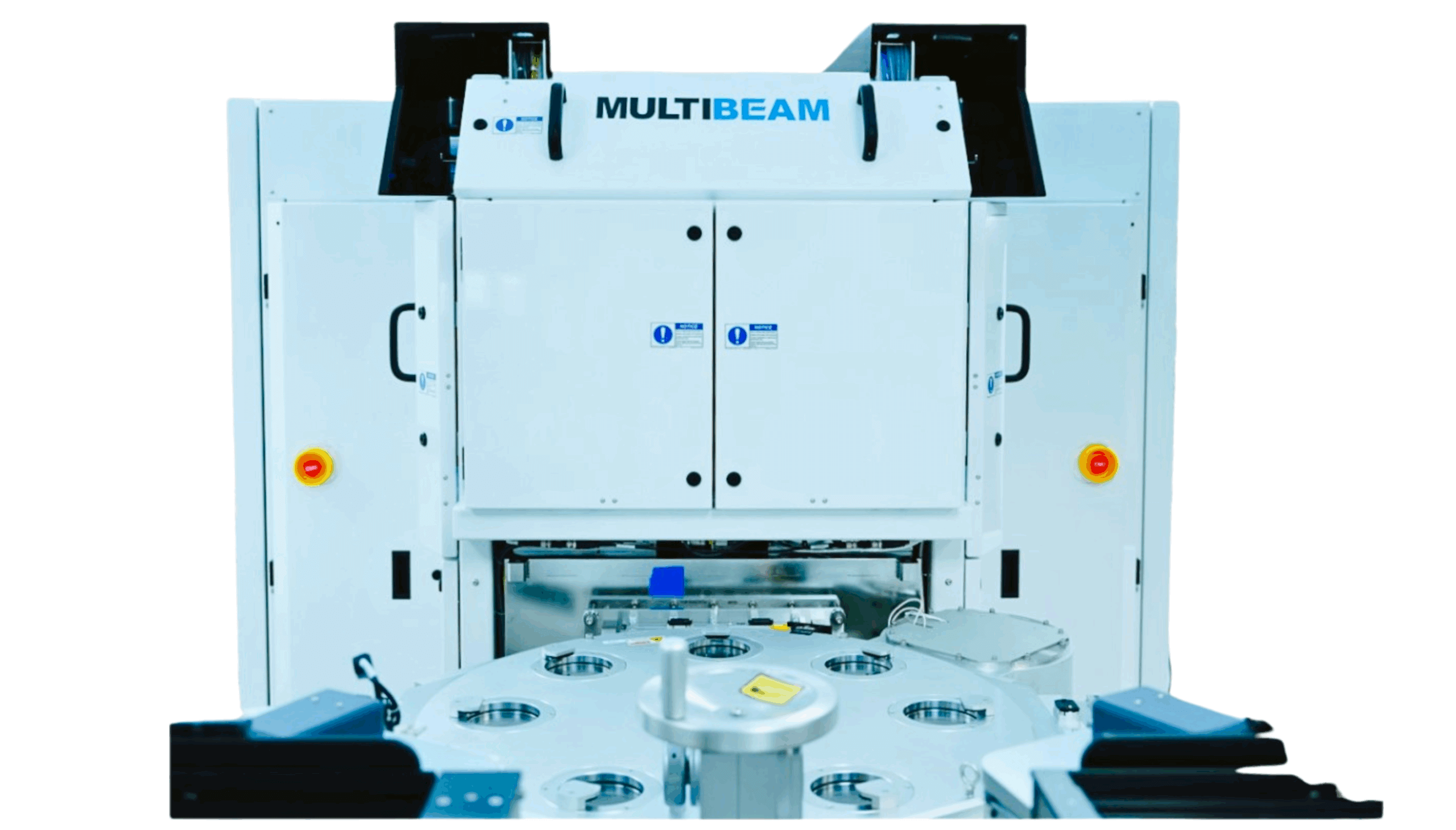
The company’s platform enables maskless, high-resolution patterning across 300mm wafers and panel-level substrates. It offers full-wafer field of view, exceptional depth of focus, and the ability to generate unique patterns. Target markets include advanced packaging, chiplet integration, quantum computing, photonics, MEMS, compound semiconductors, and power devices. Multibeam plans to use the new funding to expand product development and support emerging applications tied to artificial intelligence and other high-performance compute workloads.
Onto Innovation CEO Michael Plisinski said sub-1µm packaging interconnects represent a critical bottleneck for chiplet architectures in the AI era, and Multibeam’s direct-write lithography could cost-effectively advance dense chip integration. Executives from Lam Research’s venture arm, UMC Capital, and MediaTek Capital all pointed to the system’s flexibility, resolution, and ability to shorten prototyping cycles as key factors in their participation.
• Series B raised $31 million, led by Onto Innovation and Lam Capital
• Additional investors: UMC Capital, MediaTek Capital, other strategic backers
• Technology: multi-column electron beam lithography (MEBL) for 300mm wafers and panel-level substrates
• Applications: advanced packaging, AI chiplet integration, quantum, photonics, MEMS, compound semiconductors, power devices
• Based in Santa Clara, California
• Differentiators: maskless writing, full-wafer field of view, deep depth of focus, rapid prototyping capabilities
“We are excited to welcome our new investors,” said Dr. David K. Lam, Multibeam’s founder and chairman. “In addition to funding, they bring experience, insight and wisdom acquired from decades of developing breakthrough technologies that advanced the global semiconductor industry.”
🌐 Why it Matters: Semiconductor scaling is increasingly driven by advanced packaging and chiplet integration rather than traditional Moore’s Law shrinkage. Multibeam’s maskless lithography platform offers a new tool for rapid innovation, potentially reshaping how chipmakers address the challenges of AI, quantum, and heterogeneous integration.
Dr. David K. Lam, founder and chairman of Multibeam, is a veteran of the semiconductor equipment industry best known as the founder and former CEO of Lam Research, which he established in 1980 and grew into a major global supplier of wafer fabrication equipment. Trained as an engineer, Lam earned his Ph.D. in chemical engineering from MIT and worked at Hewlett-Packard and Xerox Palo Alto Research Center (PARC) before starting Lam Research. Over the decades, he has served as a mentor and investor in multiple Silicon Valley startups, focusing on semiconductor process technologies and advanced manufacturing. At Multibeam, Lam is applying his deep expertise in lithography and process control to develop production-ready electron beam solutions for next-generation chip applications.
🌐 We’re tracking the latest developments in networking silicon. Follow our ongoing coverage at: https://convergedigest.com/category/semiconductors/