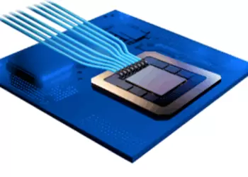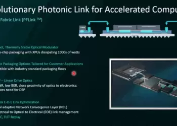
Avicena sees a huge opportunity to reshape AI cluster design with its microLED-based interconnects, a technology it says could slash energy use while breaking through the short-reach limits of copper. Speaking at this week’s IEEE Hot Interconnects online conference, Chris Pfistner, head of sales and marketing, described how the company’s “LightBundle” approach targets the dense, power-hungry connections inside scale-up networks—an area projected to become a major choke point as GPU clusters expand.
Pfistner warned that without more efficient interconnects, AI infrastructure could consume up to 20% of global energy by 2030. Today’s leading systems, such as Nvidia’s DGX, still rely on thousands of short copper cables, capped at about one meter. Avicena’s solution promises sub-1 pJ/bit energy efficiency, shoreline density above 1 Tbps/mm, and reach extended to 20 meters—all while maintaining reliability at operating temperatures up to 125°C. By leveraging GaN microLEDs from the display industry, the company also aims to drive costs well below those of laser-based silicon photonics.
The roadmap begins with a demo kit in 2025, followed by a 1.6 Tbps active optical cable in 2026 and high-density pluggables scaling up to 12.8 Tbps by 2027–28. Co-packaged optics and optical memory interconnects are planned by 2030, with test results already showing up to 20x better energy efficiency than silicon photonics.
• Energy efficiency: <1 pJ/bit (NRZ)
• Shoreline density: >1 Tbps/mm (2D arrays)
• Reach: 10–20m, up to 30m with lower efficiency
• Reliability: 10 FIT
• Operating temperature: –55°C to 125°C; tested up to 400°C
• Roadmap: Demo kit (2025), 1.6T AOC (2026), 12.8T HD pluggables (2027–28), CPO and optical memory interconnects (2030)
“Avicena’s microLED-based interconnects provide the energy efficiency and reach that AI scale-up networks urgently need,” Pfistner said.


🌐 Analysis: Avicena is adapting microLEDs, proven in the display sector, into a new class of data center interconnects. Positioned between copper and conventional optics, the approach offers low energy, low cost, and scalable reach, making it especially relevant as GPUs trend toward 2000 W+ power envelopes. Early deployments will likely come as active optical cables and high-density pluggables, but the long-term play is in co-packaged optics and optical memory links. Based in Sunnyvale, California and founded in 2019, Avicena has secured backing from Samsung Catalyst, Micron Ventures, and others. If its technology scales, it could provide a disruptive alternative to silicon photonics in hyperscale AI data centers.
🌐 We’re tracking the latest developments in networking silicon. Follow our ongoing coverage at: https://convergedigest.com/category/semiconductors/