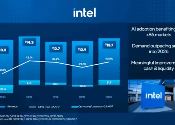
Intel outlined the architecture behind its upcoming Lunar Lake processors expected later this year. The design promises new benchmarks for performance and power management thanks to an integrated controller, enhanced Thread Director, memory-side cache and improved E-core cluster.
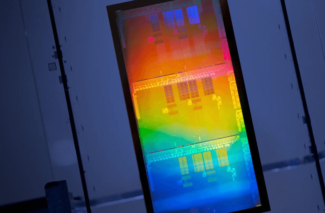
Lunar Lake’s microarchitecture consists of two unique tiles connected through Intel’s Foveros packaging technology, as well as memory on package:
Compute Tile – A new compute tile contains the latest-generation Efficient-cores (E-cores) and Performance-cores (P-cores), both of which introduce new microarchitecture enhancements and together bring unprecedented x86 efficiency. Also housed on the compute tile are the new Xe2 graphics processing unit (GPU), neural processing unit (NPU 4) and image processing unit (IPU).
- Xe2 GPU – Brings more than 80% more gaming performance and more than five times the AI throughput over the previous generation, delivering more than 60 tera-operations per second (TOPS) New microarchitecture for the display and media engines delivers a best-in-class visual experience.
- NPU 4 – Delivers three times more TOPS over the most recent generation, up to 48 TOPs, to accelerate AI computations with impressively low power.
- IPU – Provides a great camera experience with reduced power.
Platform Controller Tile (PCT) – The PCT is where security and connectivity are integrated. Security components deliver a robust integrated security solution with built-in security engines designed to establish a solid foundation for system protection. The upgraded connectivity suite integrates Wi-Fi 7.0, Bluetooth 5.4, PCIe Gen5 and PCIe Gen4 ports, and Thunderbolt 4 ports.
Memory on Package – Enables fast access to data and reduces latency, decreasing the overall power consumption of the system.
https://download.intel.com/newsroom/2024/client-computing/Lunar-Lake-Architecture-Fact-Sheet.pdf
About Intel Foveros
Intel’s Foveros packaging technology enables the stacking of multiple logic chips on top of each other, creating a more compact and efficient package. Foveros allows different types of processor cores to be integrated within a single package, improving performance, power efficiency, and form factor flexibility.
The implementation of Foveros technology involves the use of through-silicon vias (TSVs) to connect multiple active layers vertically. This method differs from traditional 2D chip designs, where components are laid out side by side. Foveros also integrates hybrid bonding techniques, enabling the combination of different process nodes and IP blocks within a single package. This approach allows for greater customization and optimization, matching specific workload requirements with tailored configurations. The ability to mix and match different chiplets enables a modular approach to chip design, which can accelerate time-to-market and reduce development costs.
Intel first announced its Foveros technology in December 2018. Since then, it has been used in various products, with the Lakefield processors being among the first to showcase its capabilities. Lakefield processors, introduced in 2020, featured a hybrid architecture with a mix of high-performance and low-power cores, demonstrating the versatility of Foveros.
- In January 2024, Intel celebrated the opening of Fab 9 in Rio Rancho, New Mexico. Fab 9 is set to play a pivotal role in driving Intel’s ongoing advancements in advanced packaging technologies. With the semiconductor industry transitioning into the heterogeneous era that embraces multiple “ chiplets ” within a single package, cutting-edge packaging technologies like Foveros and EMIB (embedded multi-die interconnect bridge) offer a swifter and more cost-effective path toward achieving the milestone of 1 trillion transistors on a single chip, extending Moore’s Law beyond 2030.