Lightmatter CEO Nick Harris took the stage at the AI Infrastructure Summit in Santa Clara to argue that the next 1000X leap in AI performance will come not from GPUs but from re-architecting the physical layer with photonic interconnects. Harris warned that chip design is hitting a “shoreline” limit—the die perimeter where I/O occurs—making communication between chips the fundamental bottleneck for scaling AI infrastructure. He contrasted decades of exponential gains in compute against only modest progress in interconnect bandwidth, leaving GPUs starved for data and data centers consuming power on the scale of cities.
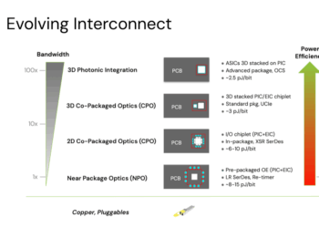
Harris outlined Lightmatter’s product roadmap aimed at breaking through these limits. The company’s L-Series integrates 3D-stacked co-packaged optics around switch and accelerator dies using wide parallel interfaces such as UCIe, while its M-Series stacks full GPUs and switches directly on a photonic substrate interposer. The flagship M1000 platform delivers 114 Tbps at 1.4 Tbps/mm² with integrated liquid cooling and 256 optical fibers, enabling kilometer-scale connectivity with 4x lower energy use than pluggables. Customers are already testing these platforms in labs, with commercial availability expected starting in 2026.
Lightmatter has announced breakthroughs in optical I/O, including an approach that packs 16 bidirectional wavelengths into a single fiber—achieving 800 Gbps per fiber at a fraction of the power cost of current pluggables. Harris positioned this as critical to scaling AI clusters into “single brain” architectures rather than today’s patchwork of smaller compute islands. He predicted that photonic interconnects will hit a crossover point at 224 Gbps per lane, beyond which copper can no longer keep pace in power or latency.
• The next 1000X leap in AI will be driven by interconnect, not compute
• Chip “shoreline” I/O limits are the primary barrier to scaling
• L-Series (3D-stacked co-packaged optics) available in 2026
• M1000 platform: 114 Tbps, 1.4 Tbps/mm², 256 fibers, 4x energy savings
• Breakthrough optical I/O: 16 bidirectional wavelengths per fiber, 800 Gbps/fiber
• Photonics expected to dominate beyond 224 Gbps per lane signaling
“Our customers are in the lab today with these platforms, and it’s safe to say they are deploying workloads that push the limits of what was thought possible even five years out,” said Harris.


🌐 Analysis: Lightmatter’s 3D stacking approach bypasses the shoreline bottleneck that constrains 2D CPO. By embedding optics beneath compute, the company addresses both bandwidth and radix scaling simultaneously—critical for trillion-parameter AI workloads. Competitors such as Ayar Labs and OpenLight are pursuing different paths in optical I/O, but Lightmatter’s microring-based density and 3D photonic interposer integration give it a distinctive position. With hyperscalers rushing to deploy AI factories at gigawatt scale, adoption of ultra-efficient photonic fabrics could determine which architectures dominate in the late 2020s.