• Home
  • Events Calendar
  • Blueprint Guidelines
  • Privacy Policy
  • Subscribe to Daily Newsletter
  • NextGenInfra.io
No Result
View All Result
Converge Digest
Monday, April 13, 2026
  • Home
  • Events Calendar
  • Blueprint Guidelines
  • Privacy Policy
  • Subscribe to Daily Newsletter
  • NextGenInfra.io
No Result
View All Result
Converge Digest
No Result
View All Result

Home » Alphawave Semi Releases 3nm UCIe Subsystem, Built on TSMC’s CoWoS

Alphawave Semi Releases 3nm UCIe Subsystem, Built on TSMC’s CoWoS

September 30, 2024
in Semiconductors
A A

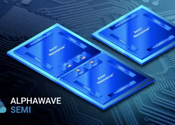
Alphawave Semi announced the availability of its 3nm silicon-proven Universal Chiplet Interconnect Express (UCIe) Die-to-Die (D2D) IP subsystem. Built on TSMC’s advanced Chip-on-Wafer-on-Substrate (CoWoS) packaging technology, this subsystem is designed for high-performance applications like hyperscale data centers, AI, and high-performance computing (HPC). The subsystem integrates both PHY and controller and provides up to 8 Tbps/mm of bandwidth density, while improving power efficiency, latency, and I/O complexity.

The UCIe IP subsystem supports multiple industry protocols including PCIe, CXL, AXI-4, AXI-S, CXS, and CHI, ensuring it fits within the evolving chiplet ecosystem. It operates at speeds of up to 24 Gbps and offers live per-lane health monitoring to enhance system robustness. Alphawave Semi has completed comprehensive testing on silicon received from TSMC, validating the subsystem’s performance under typical, slow, and fast conditions, and at different voltage and temperature ranges.

With full compliance to UCIe Specification Rev 2.0, the subsystem also includes JTAG, BIST, DFT, and Known Good Die (KGD) capabilities for testing and debugging. This release marks another step in Alphawave Semi’s strategic roadmap for delivering advanced connectivity solutions for next-generation semiconductor designs.

Key points:

• 3nm UCIe Die-to-Die IP subsystem now available.

• Built on TSMC’s Chip-on-Wafer-on-Substrate (CoWoS) advanced packaging.

• Bandwidth density of 8 Tbps/mm, supporting speeds up to 24 Gbps.

• Multiple protocol support: PCIe, CXL, AXI-4, AXI-S, CXS, and CHI.

• Includes JTAG, BIST, DFT, and Known Good Die (KGD) capabilities.

TSMC’s Chip-on-Wafer-on-Substrate (CoWoS) is a 3D stacked packaging solution that enables the integration of multiple chips, including CPUs, GPUs, memory, and other components, onto a single substrate.

“Achieving successful silicon validation of 3nm 24 Gbps UCIe subsystem with TSMC’s advanced packaging is a significant milestone for Alphawave Semi and underscores the company’s expertise in utilizing the TSMC 3DFabric™ ecosystem to deliver top-tier connectivity solutions,” said Mohit Gupta, Alphawave Semi’s SVP and GM, Custom Silicon and IP.

Tags: Alphawave SemiUCIe
ShareTweetShare
Previous Post

Verizon Sells $3.3B in Tower Rights to Vertical Bridge

Next Post

Corning Introduces a New Material for EUV Chipmaking

Jim Carroll

Jim Carroll

Editor and Publisher, Converge! Network Digest, Optical Networks Daily - Covering the full stack of network convergence from Silicon Valley

Related Posts

Polar Semi lands funding to become US-owned merchant fab
Semiconductors

Alphawave Semi Tapes Out 64 Gbps UCIe Gen3 on TSMC 3nm

September 24, 2025
Hot Interconnects: UCIe Brings On-Package Memory to the Forefront
All

Hot Interconnects: UCIe Brings On-Package Memory to the Forefront

August 22, 2025
Universal Chiplet Interconnect Express 2.0 Spec Released
All

Universal Chiplet Interconnect Express 2.0 Spec Released

August 6, 2024
Alphawave Semi collaborates with Arm on compute chiplets
All

Alphawave Semi Rides AI Wave with Record Q2 Bookings

July 24, 2024
Next Post
Corning Introduces a New Material for EUV Chipmaking

Corning Introduces a New Material for EUV Chipmaking

Categories

  • 5G / 6G / Wi-Fi
  • AI Infrastructure
  • All
  • Automotive Networking
  • Blueprints
  • Clouds and Carriers
  • Data Centers
  • Enterprise
  • Explainer
  • Feature
  • Financials
  • Last Mile / Middle Mile
  • Legal / Regulatory
  • Optical
  • Quantum
  • Research
  • Security
  • Semiconductors
  • Space
  • Start-ups
  • Subsea
  • Sustainability
  • Video
  • Webinars

Archives

Tags

5G All AT&T Australia AWS Blueprint columns BroadbandWireless Broadcom China Ciena Cisco Data Centers Dell'Oro Ericsson FCC Financial Financials Huawei Infinera Intel Japan Juniper Last Mile Last Mille LTE Mergers and Acquisitions Mobile NFV Nokia Optical Packet Systems PacketVoice People Regulatory Satellite SDN Service Providers Silicon Silicon Valley StandardsWatch Storage TTP UK Verizon Wi-Fi
Converge Digest

A private dossier for networking and telecoms

Follow Us

  • Home
  • Events Calendar
  • Blueprint Guidelines
  • Privacy Policy
  • Subscribe to Daily Newsletter
  • NextGenInfra.io

© 2025 Converge Digest - A private dossier for networking and telecoms.

No Result
View All Result
  • Home
  • Events Calendar
  • Blueprint Guidelines
  • Privacy Policy
  • Subscribe to Daily Newsletter
  • NextGenInfra.io

© 2025 Converge Digest - A private dossier for networking and telecoms.

This website uses cookies. By continuing to use this website you are giving consent to cookies being used. Visit our Privacy and Cookie Policy.
Go to mobile version