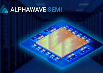
Alphawave Semi announced the tapeout of its 64 Gbps UCIe Gen3 IP subsystem on TSMC’s 3nm (N3P) process, setting a new benchmark for die-to-die connectivity in chiplet-based architectures. The design doubles shoreline bandwidth density compared to prior generations and reaches up to 3.6 Tbps/mm in standard packaging, with more than 21 Tbps/mm in advanced configurations. The subsystem supports scalable XPUs and data center SoCs, providing the foundation for AI infrastructure requiring higher lane counts and energy efficiency.
The 64 Gbps UCIe IP delivers interoperability across chiplets, with integrated protocol support for AXI-4, AXI-S, CXS, and CHI, while enabling advanced testing features such as BIST, DFT, iJTAG, Known Good Die validation, and live per-lane monitoring. Alphawave positions the subsystem as a building block for custom memory interfaces and Co-Packaged Optics (CPO), offering up to eight times the bandwidth density of traditional memory connections. Compliance with UCIe 3.0, released in August 2025, ensures alignment with the evolving industry standard.
Alphawave Semi said this marks a critical step in its progression from 36 Gbps to 64 Gbps UCIe IP, reinforcing its AI platform strategy and chiplet reference architecture. “The industry’s first tapeout of our Gen3 UCIe™ IP at 64 Gbps on TSMC’s N3P process marks a significant leap forward in die-to-die connectivity,” said Mohit Gupta, EVP & GM at Alphawave Semi. “It strengthens our broader AI platform—ensuring our suite of IP subsystems now delivers higher performance and efficiency than ever before.”
• First 64 Gbps UCIe Gen3 IP subsystem taped-out on TSMC 3nm
• Delivers up to 3.6 Tbps/mm shoreline bandwidth (standard) and 21 Tbps/mm (advanced)
• Supports AXI-4, AXI-S, CXS, CHI, and CHI C2C protocols for flexible chiplet integration
• Fully compliant with UCIe 3.0 standard (August 2025 release)
• Enables custom memory interfaces and Co-Packaged Optics for AI data centers
🌐 Analysis: This milestone strengthens Alphawave Semi’s role in shaping the UCIe ecosystem, a critical enabler for chiplet-based AI infrastructure. The leap from 36 Gbps to 64 Gbps on TSMC’s 3nm node highlights both foundry and IP ecosystem collaboration. Competitors such as Synopsys and Cadence are also advancing UCIe portfolios, but Alphawave’s early tapeout at 64 Gbps positions it as a key player in meeting hyperscaler demands for high-bandwidth, low-power die-to-die connectivity.
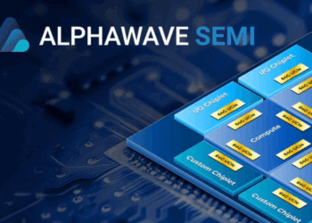
Universal Chiplet Interconnect Express (UCIe) is an open industry standard for die-to-die (D2D) interconnect, designed to enable multi-vendor chiplet ecosystems. Established in March 2022, the UCIe Consortium brings together leading semiconductor, foundry, and systems companies to standardize how chiplets from different vendors communicate inside a package. The goal is to provide the same level of interoperability and scalability for chiplets that PCIe delivers for boards and systems.
At its core, UCIe defines the physical layer, die-to-die protocols, and software stack required to integrate compute, memory, and I/O chiplets. By supporting both short-reach (standard package) and ultra-short-reach (advanced package) connections, UCIe allows designers to scale bandwidth density while lowering power consumption. This approach enables disaggregated SoC architectures, where functionality can be mixed and matched—CPU, GPU, memory, and accelerators—without the cost and yield penalties of monolithic dies at advanced process nodes.
The specification has evolved quickly. UCIe 1.0 (2022) provided the initial framework for die-to-die PHY and protocol stack. UCIe 2.0 (2023) added improvements in bandwidth efficiency, latency, and reliability features. UCIe 3.0, released in August 2025, introduced support for higher per-pin data rates (up to 64 Gbps) and enhancements for CXL, PCIe, and custom memory interfaces, enabling the next wave of chiplet adoption in AI and hyperscale data centers.
Why UCIe Matters
- Standardizes die-to-die connectivity across vendors, reducing ecosystem fragmentation
- Supports both standard organic substrates and advanced packaging (e.g., silicon interposers, 3D stacking)
- Scales to >20 Tbps/mm shoreline bandwidth in advanced implementations
- Optimizes for low power and low latency—critical for AI, HPC, and data center workloads
- Provides test, debug, and Known Good Die (KGD) features for reliable multi-die integration
UCIe Version Roadmap
| Version | Release Date | Key Features |
|---|---|---|
| UCIe 1.0 | March 2022 | • Initial specification • Standard die-to-die PHY and protocol stack • Support for PCIe & CXL tunneling • Short-reach (standard pkg) & ultra-short reach (advanced pkg) |
| UCIe 2.0 | June 2023 | • Improved bandwidth efficiency & latency • Reliability & error-handling features • Extended test/diagnostics (DFT, KGD) • Wider ecosystem adoption |
| UCIe 3.0 | August 2025 | • Up to 64 Gbps per I/O pin • Shoreline bandwidth density >20 Tbps/mm (advanced) • Enhanced support for PCIe, CXL, and custom memory interfaces • Roadmap toward optical chiplet integration & CPO |
Source: UCIe Consortium
🌐 We’re tracking the latest developments in networking silicon. Follow our ongoing coverage at: https://convergedigest.com/category/semiconductors/