• Home
  • Events Calendar
  • Blueprint Guidelines
  • Privacy Policy
  • Subscribe to Daily Newsletter
  • NextGenInfra.io
No Result
View All Result
Converge Digest
Friday, April 10, 2026
  • Home
  • Events Calendar
  • Blueprint Guidelines
  • Privacy Policy
  • Subscribe to Daily Newsletter
  • NextGenInfra.io
No Result
View All Result
Converge Digest
No Result
View All Result

Home » Alphawave Semi Tapes Out UCIe 3D Chiplet on TSMC

Alphawave Semi Tapes Out UCIe 3D Chiplet on TSMC

October 1, 2025
in Semiconductors
A A

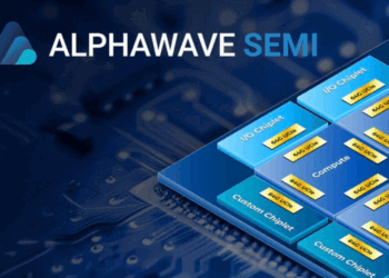
Alphawave Semi has completed the tape-out of its next-generation UCIe™ 3D chiplet IP on TSMC’s SoIC-X technology, part of the foundry’s 3DFabric® platform. This marks a significant step in advancing 3D integration for high-performance compute (HPC) and AI workloads. The new IP enables face-to-face (F2F) die stacking, providing up to 10x power efficiency and 5x signal density improvements compared to traditional 2.5D die-to-die interfaces.

The 3D architecture features a 5nm bottom die with through-silicon vias (TSVs) to support a 3nm top die, using Alphawave Semi’s proprietary 3DIO design methodology. This approach addresses critical bottlenecks in memory bandwidth and power delivery as monolithic SoC scaling slows. Alphawave’s work aligns with broader industry trends favoring disaggregated architectures and vertical integration via advanced packaging.

The announcement builds on a prior tape-out of UCIe IP on TSMC’s 2nm CoWoS® platform and supports the company’s roadmap to deliver UCIe with 64G support. Strategic collaboration with Siemens and TSMC reinforces Alphawave’s ecosystem positioning as a key enabler for chiplet-based AI and HPC systems.

  • Delivers 10x power efficiency and 5x signal density over traditional 2.5D interfaces
  • Supports F2F die stacking with 5nm-to-3nm TSV integration
  • Built on TSMC’s SoIC-X 3DFabric advanced 3D packaging platform
  • Part of Alphawave’s growing 3DIO IP portfolio for AI and HPC
  • Collaborations announced with Siemens and TSMC under OIP program
  • Builds on Alphawave’s 2nm UCIe IP tape-out on TSMC CoWoS® in June
  • Future roadmap includes 64G UCIe support for next-gen chiplet systems

“This successful tape-out represents a significant milestone for Alphawave Semi and our AI platform,” said Mohit Gupta, EVP & GM at Alphawave Semi. “By combining our high-speed 3D UCIe IP with TSMC’s groundbreaking SoIC-X technology, we are directly addressing the memory and bandwidth bottlenecks that limit our customers’ next-generation AI and HPC applications.”

🌐 Analysis: The push toward UCIe-based chiplet systems has become a central theme in the race to scale AI infrastructure, especially as traditional monolithic SoC integration hits limits. Alphawave Semi’s latest achievement highlights the importance of TSMC’s 3DFabric technologies, which have gained traction among advanced silicon players. With partners like Intel, AMD, Broadcom, and NVIDIA also exploring UCIe, the ecosystem is rapidly coalescing around standardized 3D die integration, and Alphawave’s early leadership in IP positions it well for the next wave of modular compute.

🌐 We’re tracking the latest developments in networking silicon. Follow our ongoing coverage at: https://convergedigest.com/category/semiconductors/

Tags: AlphawaveChipletTSMC
ShareTweetShare
Previous Post

Meta Acquires Rivos for RISC-V and AI Acceleration

Next Post

Credo Acquires Hyperlume for MicroLED Optical Interconnect 

Jim Carroll

Jim Carroll

Editor and Publisher, Converge! Network Digest, Optical Networks Daily - Covering the full stack of network convergence from Silicon Valley

Related Posts

Tenstorrent Launches Open Chiplet Atlas Ecosystem
Semiconductors

Tenstorrent Launches Open Chiplet Atlas Ecosystem

October 24, 2025
ECOC25: Alphawave Semi Shows 224G SerDes and Optical Chiplets
Optical

ECOC25: Alphawave Semi Shows 224G SerDes and Optical Chiplets

September 29, 2025
Alchip and Ayar Labs Team on Co-Packaged Optics
All

Alchip and Ayar Labs Team on Co-Packaged Optics

September 26, 2025
Cadence Expands TSMC Partnership with AI-Driven Design
Semiconductors

Cadence Expands TSMC Partnership with AI-Driven Design

September 25, 2025
Polar Semi lands funding to become US-owned merchant fab
Semiconductors

Alphawave Semi Tapes Out 64 Gbps UCIe Gen3 on TSMC 3nm

September 24, 2025
Polar Semi lands funding to become US-owned merchant fab
Semiconductors

AMD Licenses Arteris FlexGen for Chiplet Designs

August 4, 2025
Next Post
Credo Acquires Hyperlume for MicroLED Optical Interconnect 

Credo Acquires Hyperlume for MicroLED Optical Interconnect 

Categories

  • 5G / 6G / Wi-Fi
  • AI Infrastructure
  • All
  • Automotive Networking
  • Blueprints
  • Clouds and Carriers
  • Data Centers
  • Enterprise
  • Explainer
  • Feature
  • Financials
  • Last Mile / Middle Mile
  • Legal / Regulatory
  • Optical
  • Quantum
  • Research
  • Security
  • Semiconductors
  • Space
  • Start-ups
  • Subsea
  • Sustainability
  • Video
  • Webinars

Archives

Tags

5G All AT&T Australia AWS Blueprint columns BroadbandWireless Broadcom China Ciena Cisco Data Centers Dell'Oro Ericsson FCC Financial Financials Huawei Infinera Intel Japan Juniper Last Mile Last Mille LTE Mergers and Acquisitions Mobile NFV Nokia Optical Packet Systems PacketVoice People Regulatory Satellite SDN Service Providers Silicon Silicon Valley StandardsWatch Storage TTP UK Verizon Wi-Fi
Converge Digest

A private dossier for networking and telecoms

Follow Us

  • Home
  • Events Calendar
  • Blueprint Guidelines
  • Privacy Policy
  • Subscribe to Daily Newsletter
  • NextGenInfra.io

© 2025 Converge Digest - A private dossier for networking and telecoms.

No Result
View All Result
  • Home
  • Events Calendar
  • Blueprint Guidelines
  • Privacy Policy
  • Subscribe to Daily Newsletter
  • NextGenInfra.io

© 2025 Converge Digest - A private dossier for networking and telecoms.

This website uses cookies. By continuing to use this website you are giving consent to cookies being used. Visit our Privacy and Cookie Policy.
Go to mobile version