• Home
  • Events Calendar
  • Blueprint Guidelines
  • Privacy Policy
  • Subscribe to Daily Newsletter
  • NextGenInfra.io
No Result
View All Result
Converge Digest
Saturday, April 11, 2026
  • Home
  • Events Calendar
  • Blueprint Guidelines
  • Privacy Policy
  • Subscribe to Daily Newsletter
  • NextGenInfra.io
No Result
View All Result
Converge Digest
No Result
View All Result

Home » Amkor Expands AZ Investment to $7B for Advanced Semiconductor Packaging Campus

Amkor Expands AZ Investment to $7B for Advanced Semiconductor Packaging Campus

October 6, 2025
in Semiconductors
A A

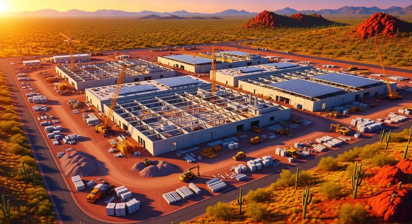
Amkor Technology has broken ground on its new advanced semiconductor packaging and test campus in Arizona, expanding its total planned investment to $7 billion. The expansion adds a second greenfield facility and additional cleanroom space, marking a significant milestone for domestic chip manufacturing. When completed, the two-phase project will comprise over 750,000 square feet of cleanroom space and employ up to 3,000 people.

The campus will be the first high-volume outsourced advanced packaging facility in the United States, designed to complement TSMC’s wafer fabrication operations in nearby Phoenix. It will serve major customers including Apple and NVIDIA, integrating smart factory technologies and scalable production for AI, high-performance computing, mobile, and automotive chips. Construction of the first phase is set to finish in mid-2027, with production ramping in early 2028. The project is backed by federal incentives under the CHIPS for America Program, the Advanced Manufacturing Investment Tax Credit, and state and local support.

“This groundbreaking represents a bold step in Amkor’s long-term strategy for growth and innovation,” said Giel Rutten, president and CEO of Amkor Technology. “We’re building a facility to meet our customers’ most advanced needs that will help shape the future of semiconductor manufacturing in the United States.”

🌐 Analysis: Arizona has become one of the most concentrated semiconductor hubs in the U.S., with major investments across the full manufacturing chain:

  • TSMC Arizona – $65 billion investment for two fabs in north Phoenix producing 3nm and 2nm chips by 2028.Intel – More than $32 billion expansion of its Ocotillo campus in Chandler, including Fab 52 and Fab 62 for advanced process nodes and packaging.Amkor Technology – $7 billion for two phases of outsourced advanced packaging and test facilities in Tempe/Peoria.Edwards Vacuum – $600 million semiconductor manufacturing component plant supporting TSMC supply chain in Chandler.Applied Materials – $2 billion Equipment and Process Innovation and Collaboration Center (EPIC) in Silicon Desert corridor.NXP Semiconductors – $290 million investment to expand RF and automotive chip capacity in Chandler.Micron Technology – Evaluating a potential Arizona site for DRAM packaging and assembly operations (unconfirmed).Lucid Motors and Onsemi – Expanding semiconductor and power electronics manufacturing in Casa Grande and East Phoenix for EV applications.

  • Together, these projects represent well over $100 billion in cumulative semiconductor-related investment across Arizona, positioning the state as the epicenter of U.S. chip fabrication, advanced packaging, and materials innovation.

    🌐 We’re tracking the latest developments in semiconductors. Follow our ongoing coverage at: https://convergedigest.com/category/semiconductors/

    Tags: AmkorArizona
    ShareTweetShare
    Previous Post

    #AINetworking25: Digging into Agentic-AI Operations with Blue Planet – Director’s Cut

    Next Post

    AMD and OpenAI Ink 6-Gigawatt GPU Deal

    Jim Carroll

    Jim Carroll

    Editor and Publisher, Converge! Network Digest, Optical Networks Daily - Covering the full stack of network convergence from Silicon Valley

    Related Posts

    Vantage Data Centers cites progress with its massive Phoenix campus
    All

    Vantage Data Centers cites progress with its massive Phoenix campus

    November 23, 2021
    Next Post
    AMD and OpenAI Ink 6-Gigawatt GPU Deal

    AMD and OpenAI Ink 6-Gigawatt GPU Deal

    Categories

    • 5G / 6G / Wi-Fi
    • AI Infrastructure
    • All
    • Automotive Networking
    • Blueprints
    • Clouds and Carriers
    • Data Centers
    • Enterprise
    • Explainer
    • Feature
    • Financials
    • Last Mile / Middle Mile
    • Legal / Regulatory
    • Optical
    • Quantum
    • Research
    • Security
    • Semiconductors
    • Space
    • Start-ups
    • Subsea
    • Sustainability
    • Video
    • Webinars

    Archives

    Tags

    5G All AT&T Australia AWS Blueprint columns BroadbandWireless Broadcom China Ciena Cisco Data Centers Dell'Oro Ericsson FCC Financial Financials Huawei Infinera Intel Japan Juniper Last Mile Last Mille LTE Mergers and Acquisitions Mobile NFV Nokia Optical Packet Systems PacketVoice People Regulatory Satellite SDN Service Providers Silicon Silicon Valley StandardsWatch Storage TTP UK Verizon Wi-Fi
    Converge Digest

    A private dossier for networking and telecoms

    Follow Us

    • Home
    • Events Calendar
    • Blueprint Guidelines
    • Privacy Policy
    • Subscribe to Daily Newsletter
    • NextGenInfra.io

    © 2025 Converge Digest - A private dossier for networking and telecoms.

    No Result
    View All Result
    • Home
    • Events Calendar
    • Blueprint Guidelines
    • Privacy Policy
    • Subscribe to Daily Newsletter
    • NextGenInfra.io

    © 2025 Converge Digest - A private dossier for networking and telecoms.

    This website uses cookies. By continuing to use this website you are giving consent to cookies being used. Visit our Privacy and Cookie Policy.
    Go to mobile version