Ayar Labs appointed Dr. Ken Chang as Senior Vice President of Engineering.
Dr. Chang is the former VP of Wired Engineering at Xilinx, where he led its SerDes technology group which delivered industry first 28G KR/CR compliant transceivers for FPGAs and 56G PAM4 and 112G PAM4 transceivers capable of long reach transmission. Prior to that, he was at Rambus for 11 years where he led the development of numerous products and advanced technology development projects, all in the high-speed links domain.
Dr. Chang, an IEEE fellow since 2018, brings a wealth of industry and research experience to Ayar Labs. He has authored or co-authored over 50 technical papers in ISSCC, VLSI, A-SSCC, and JSSC in the area of chip-to-chip interfaces and chip-to-memory. He is also active in the IEEE community and recently served as the technical program chair and co-chair of the VLSI Circuit Symposium in 2018 and 2017, respectively, and served on the Technical Program Committee since 2009. He also served on the Technical Program Committee of ISSCC from 2011-2016 and CICC from 2008-2010.
“We’re excited to have Dr. Ken Chang join Ayar Labs to lead our growing engineering organization,” said Charles Wuischpard, CEO of Ayar Labs. “Ken has decades of experience in bringing high speed I/O products to market as well as leading and growing world class engineering organizations. He joins Ayar Labs at a seminal moment as the industry prepares to transition to in-package optical I/O to meet growing workload demands and maintain Moore’s Law scaling.”
“I believe that silicon photonics is critical for the advancement of high-performance interconnects,” said Dr. Chang. “Ayar Labs has pioneered much of the technology for in-package optical I/O through its development of micro-ring resonator-based electro-optical chiplets that deliver the bandwidth density and energy efficiency in cost effective 2.5/3D packaging solutions to make this future a reality. I am excited to join this very talented and energetic team to bring these transformative innovations to market.”
yar Labs hits key milestone for chip-to-chip optical connectivity
Ayar Labs demonstrated its patented monolithic electronic/photonic solution on Globalfoundries’ next-gen photonics solution based on its 45nm platform.
The companies said this industry-first demonstration is a key milestone in providing chip-to-chip optical connectivity at scale. The two companies began working together in 2015 with a commitment to collaborate and commercialize differentiated silicon photonics solutions for greenfield applications that would require extreme bandwidth density (high data throughput in a small physical package) at low latency and high energy efficiency.
“Ayar Labs has been perfecting our micro-ring based monolithic electronic/photonic solution for nearly a decade. But the true commercial potential is realized when coupled with a 300mm semiconductor fabrication process that delivers the performance, reliability, and cost advantages that we and our customers require,” says Charles Wuischpard, CEO, Ayar Labs. “This is yet another industry-first result that solidifies our leadership for this market opportunity.”
“Ayar Labs is an important partner of GLOBALFOUNDRIES,” says Anthony Yu, Vice President of Silicon Photonics at GF. “As collaborators, we’ve incorporated their requirements for PDK and process optimizations while providing early access to our next-generation process. Together, we will unlock a larger market opportunity and realize chip-to-chip optical I/O solutions that will enable higher bandwidth and faster connection for high performance compute applications.”

Over the last 18 months, Ayar Labs has been working with select semiconductor manufacturers, systems builders, and end users on co-design partnerships. The company is now announcing an expanded sampling program of its next-generation chiplet developed on GF’s latest silicon photonics manufacturing process that will be available to a broader group by request at ayarlabs.com/starterkit/
Dr. Mark Wade, President and CTO of Ayar Labs, will be sharing details of this industry first demonstration at ECOC 2020 as part of his presentation on ‘Silicon photonic chiplets for chip-to-chip communications’ on Tuesday, December 8, from 16:20 – 16:40 (CET). A video of the demonstration will also be made available at this time.
Lockheed Martin Ventures invests in Ayar Labs
Lockheed Martin Ventures has made a strategic investment in Ayar Labs, a start-up that is developing monolithic in-package optical I/O (MIPO) solution for applications that require high bandwidth, low latency and power efficient short reach interconnects. Financial terms were not disclosed.
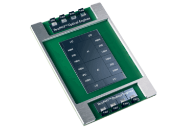
Ayar Labs publicly demonstrated its monolithic electronic photonic TeraPHY chiplet at the Supercomputing 2019 conference and is now working with select semiconductor manufacturers, OEM systems builders, and end users on sampling and co-design partnerships in 2020. The company is based in Santa Clara, California.
“We are excited to welcome Lockheed Martin Ventures as a strategic investor,” said Charles Wuischpard, CEO of Ayar Labs. “Working with key system integrators like Lockheed Martin, who really understand the value of our solution and how to design it into future complex systems, is incredibly important. In that sense, we view this relationship as more than funding alone, but as an important long-term working relationship as well.”
Ayar Labs selected for Intel’s DARPA PIPES Project
Ayar Labs has been selected as Intel’s optical I/O solution partner for their recently awarded DARPA PIPES (Photonics in Package for Extreme Scalability) project.
The PIPES project aims to develop integrated optical I/O solutions co-packaged with next generation FPGA/CPU/GPU and accelerators in Multi-Chip Packages (MCP) to provide extreme data rates (input/output) at ultra-low power over much longer distances than supported by current technology. In the first phase of the project, the Ayar Labs TeraPHY chiplet will be co-packaged with an Intel FPGA using the AIB (Advanced Interconnect Bus) interface and Intel’s EMIB silicon-bridge packaging. “We’re seeing an explosion of Datacenter workloads that have an insatiable demand for bandwidth and the need to connect devices at rack-scale distances,” said Vince Hu, VP of Strategy and Innovation for Intel’s FPGA products. “The best way to do that is with optical interconnect and by using an Ayar Labs chiplet(s), we can achieve very high bandwidth at low latency and low power consumption.”