• Home
  • Events Calendar
  • Blueprint Guidelines
  • Privacy Policy
  • Subscribe to Daily Newsletter
  • NextGenInfra.io
No Result
View All Result
Converge Digest
Saturday, April 11, 2026
  • Home
  • Events Calendar
  • Blueprint Guidelines
  • Privacy Policy
  • Subscribe to Daily Newsletter
  • NextGenInfra.io
No Result
View All Result
Converge Digest
No Result
View All Result

Home » Ayar Labs selected for Intel’s DARPA PIPES Project

Ayar Labs selected for Intel’s DARPA PIPES Project

November 21, 2019
in All
A A

Ayar Labs has been selected as Intel’s optical I/O solution partner for their recently awarded DARPA PIPES (Photonics in Package for Extreme Scalability) project.

The PIPES project aims to develop integrated optical I/O solutions co-packaged with next generation FPGA/CPU/GPU and accelerators in Multi-Chip Packages (MCP) to provide extreme data rates (input/output) at ultra-low power over much longer distances than supported by current technology. In the first phase of the project, the Ayar Labs TeraPHY chiplet will be co-packaged with an Intel FPGA using the AIB (Advanced Interconnect Bus) interface and Intel’s EMIB silicon-bridge packaging. “We’re seeing an explosion of Datacenter workloads that have an insatiable demand for bandwidth and the need to connect devices at rack-scale distances,” said Vince Hu, VP of Strategy and Innovation for Intel’s FPGA products. “The best way to do that is with optical interconnect and by using an Ayar Labs chiplet(s), we can achieve very high bandwidth at low latency and low power consumption.”

“Bringing optical connectivity all the way into the CPU/SOC package has long been one of the ‘Holy Grail’ projects in High Performance and Hyperscale Computing, as it unleashes the performance of ever more powerful computing and network processors and removes a major bottleneck and set of constraints in systems architecture and design,” said Charles Wuischpard, CEO of Ayar Labs, “Moreover, the energy consumed in moving data through a system is now very significant and growing, and the best way to manage that is to move the data optically from end to end. We are pleased to be selected by Intel as the optical solution for their DARPA PIPES project and look forward to a multi-year collaboration.”

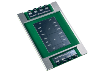
The TeraPHY chiplet is manufactured on GLOBALFOUNDRIES’ 45nm platform, which enabled Ayar Labs to build a monolithic, single-die solution that integrates both electrical and optical photonic circuits and devices on a single chip.

“We have worked in close collaboration with Ayar Labs to deliver a new class of integrated electronic, photonics solutions,” said Anthony Yu, vice president of Computing and Wired Infrastructure at GF. “Going forward, we’re excited to work with the pioneers at Ayar Labs to continue disrupting the market by combining our next generation 45nm platform, targeted to future CMOS-based photonics solutions, with their differentiated technology that will push the limits of chip communication bandwidth for high-performance computing, cloud and AI applications.”

Ayar Labs also announced customer sampling of its fully integrated TeraPHY chiplet starting in early Q1 2020.

http://www.ayarlabs.com

Tags: AyarBlueprint columnsDARPA
ShareTweetShare
Previous Post

Credo Joins Open Compute Project (OCP) to Accelerate 400G

Next Post

Spectra7 and Molex showcase 400G Active Copper Interconnects

Staff

Staff

Related Posts

Alchip and Ayar Labs Team on Co-Packaged Optics
Optical

Ayar Labs hires ex-Google executive Vivek Gupta as CSO

October 9, 2025
DARPA Demonstrates 800W Optical Power Beaming Over 8.6 Kilometers
Optical

DARPA Demonstrates 800W Optical Power Beaming Over 8.6 Kilometers

May 21, 2025
NIST Finalizes Quantum-Resistant Encryption Standards
Quantum

DARPA Selects Nearly 20 Companies for Quantum Benchmarking Initiative

April 6, 2025
Ayar Labs Launches UCIe Optical Chiplet
All

Ayar Labs Launches UCIe Optical Chiplet

April 3, 2025
BBN Developing Photonic Chip Quantum Sensors under DARPA’s INSPIRED
Optical

BBN Developing Photonic Chip Quantum Sensors under DARPA’s INSPIRED

December 4, 2024
Taiwan’s GlobalWafer lands $400M in CHIPs Act funding for Texas fab
Semiconductors

DARPA Awards $10.2M Contract to HexaTech for 100 mm AlN Substrate 

October 2, 2024
Next Post
Spectra7 and Molex showcase 400G Active Copper Interconnects

Spectra7 and Molex showcase 400G Active Copper Interconnects

Please login to join discussion

Categories

  • 5G / 6G / Wi-Fi
  • AI Infrastructure
  • All
  • Automotive Networking
  • Blueprints
  • Clouds and Carriers
  • Data Centers
  • Enterprise
  • Explainer
  • Feature
  • Financials
  • Last Mile / Middle Mile
  • Legal / Regulatory
  • Optical
  • Quantum
  • Research
  • Security
  • Semiconductors
  • Space
  • Start-ups
  • Subsea
  • Sustainability
  • Video
  • Webinars

Archives

Tags

5G All AT&T Australia AWS Blueprint columns BroadbandWireless Broadcom China Ciena Cisco Data Centers Dell'Oro Ericsson FCC Financial Financials Huawei Infinera Intel Japan Juniper Last Mile Last Mille LTE Mergers and Acquisitions Mobile NFV Nokia Optical Packet Systems PacketVoice People Regulatory Satellite SDN Service Providers Silicon Silicon Valley StandardsWatch Storage TTP UK Verizon Wi-Fi
Converge Digest

A private dossier for networking and telecoms

Follow Us

  • Home
  • Events Calendar
  • Blueprint Guidelines
  • Privacy Policy
  • Subscribe to Daily Newsletter
  • NextGenInfra.io

© 2025 Converge Digest - A private dossier for networking and telecoms.

No Result
View All Result
  • Home
  • Events Calendar
  • Blueprint Guidelines
  • Privacy Policy
  • Subscribe to Daily Newsletter
  • NextGenInfra.io

© 2025 Converge Digest - A private dossier for networking and telecoms.

This website uses cookies. By continuing to use this website you are giving consent to cookies being used. Visit our Privacy and Cookie Policy.
Go to mobile version