Cadence introduced the industry’s first DDR5 12.8Gbps MRDIMM Gen2 memory IP system solution on TSMC’s N3 process node, targeting AI, HPC, and data center workloads that demand high bandwidth and low latency. The new solution, already in use by major AI and enterprise customers, delivers a full memory subsystem—including a high-speed PHY and controller—optimized for the next generation of SoCs and chiplets.
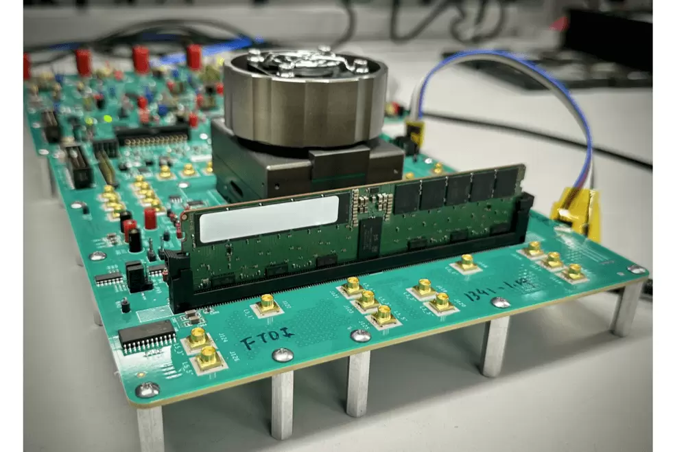
Designed to operate with Gen2 MRDIMM modules, the Cadence DDR5 IP achieves a 12.8Gbps data rate—double the bandwidth of conventional DDR5-6400 interfaces. It incorporates silicon-proven design elements from Cadence’s DDR5 and GDDR6 product families and offers fine-grained power/performance tuning, low-latency encryption, and advanced reliability, availability, and serviceability (RAS) features. The system solution has also been validated using Montage Technology’s MRCD02/MDB02 memory buffers and Micron’s 1-gamma DRAM.
To ensure rapid development cycles, Cadence has verified the controller and PHY with its own Verification IP (VIP) for DDR5, including system-level analysis capabilities. The solution provides a critical memory infrastructure component for future-proofing compute architectures focused on AI/ML inference, cloud data analytics, and memory-hungry enterprise applications.
- Cadence launches the first DDR5 12.8Gbps MRDIMM Gen2 IP on TSMC N3 for AI and HPC.
- Supports 12.8Gbps data rates, doubling bandwidth over standard DDR5-6400 memory.
- Offers complete memory subsystem with PHY, controller, low-latency encryption, and RAS features.
- Verified with Micron 1γ DRAM and Montage MRDIMM buffer chips (MRCD02/MDB02).
- Includes full Cadence Verification IP (VIP) suite for rapid IP and SoC-level validation.
“This new leading-edge memory IP system both raises the bar and establishes a roadmap that future-proofs our customers’ next-generation SoC and chiplet products for generations to come,” said Boyd Phelps, SVP and GM of the Silicon Solutions Group at Cadence.