• Home
  • Events Calendar
  • Blueprint Guidelines
  • Privacy Policy
  • Subscribe to Daily Newsletter
  • NextGenInfra.io
No Result
View All Result
Converge Digest
Friday, April 10, 2026
  • Home
  • Events Calendar
  • Blueprint Guidelines
  • Privacy Policy
  • Subscribe to Daily Newsletter
  • NextGenInfra.io
No Result
View All Result
Converge Digest
No Result
View All Result

Home » Cadence Expands TSMC Partnership with AI-Driven Design

Cadence Expands TSMC Partnership with AI-Driven Design

September 25, 2025
in Semiconductors
A A

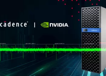
Cadence announced a major expansion of its collaboration with TSMC to accelerate AI and HPC semiconductor design, covering advanced EDA flows, 3D-IC packaging, and high-performance IP. The partnership spans process nodes from N3 to N2 and A16, with early work already underway for TSMC’s A14 process. The companies said these updates will streamline time-to-market for customers deploying AI-driven design methodologies.

Cadence confirmed that its AI-enabled design tools, including the JedAI platform, Cerebrus Intelligent Chip Explorer, and Innovus+ AI Assistant, are validated for TSMC’s N2 process. These flows bring automation for DRC violation fixing and improved power, performance, and area optimization. On the 3D-IC side, Cadence tools now support TSMC’s 3DFabric packaging ecosystem, adding automation for bump connections, chiplet placement, and thermal simulation techniques tied to the TSMC Compact Universal Photonic Engine (TSMC-COUPE).

On the IP front, Cadence introduced silicon-proven offerings on TSMC N3P, including the first HBM4 IP, high-speed LPDDR6/5X and DDR5 MRDIMM Gen2 memory interfaces, PCIe 7.0 at 128GT/s, a 224G SerDes, eUSB2V2, and 32G UCIe IP. These solutions target bandwidth and interconnect challenges for next-generation AI infrastructure and chiplet ecosystems.

• Cadence AI design flows validated for TSMC N3, N2, and A16, with A14 PDK due later this year

• AI-driven automation improves productivity for N2 node chip design

• 3D-IC tools enhanced for TSMC 3DFabric, including chiplet and photonic integration support

• New IP on N3P includes HBM4, LPDDR6/5X, DDR5 MRDIMM Gen2, PCIe 7.0, 224G SerDes, UCIe 32G, and eUSB2V2

• Focus on AI, HPC, and emerging AI PC workloads

“Cadence and TSMC remain committed to speeding up and improving the design process for advanced silicon for our customers,” said Chin-Chi Teng, senior vice president and general manager of the Digital and Signoff Group at Cadence.

🌐 Analysis: Cadence’s deepened integration with TSMC underscores the growing importance of AI-driven design tools and chiplet-based architectures in AI infrastructure. The addition of validated flows at N2 and silicon-proven IP at N3P positions Cadence strongly against rivals Synopsys and Siemens, who are also racing to enable design automation and IP for AI workloads. The extension of work into TSMC’s A14 process indicates both firms’ urgency in preparing the design ecosystem ahead of customer tapeouts in the coming technology nodes.

🌐 We’re tracking the latest developments in networking silicon. Follow our ongoing coverage at: https://convergedigest.com/category/semiconductors/

Tags: CadenceTSMC
ShareTweetShare
Previous Post

OpenAI, Oracle, SoftBank Unveil 5 New Stargate AI Data Center Sites

Next Post

Huawei Targets Subsea + Terrestrial with 100T Platform, 1.6T SLTE

Jim Carroll

Jim Carroll

Editor and Publisher, Converge! Network Digest, Optical Networks Daily - Covering the full stack of network convergence from Silicon Valley

Related Posts

Alphawave Semi Tapes Out UCIe 3D Chiplet on TSMC
Semiconductors

Alphawave Semi Tapes Out UCIe 3D Chiplet on TSMC

October 1, 2025
Alchip and Ayar Labs Team on Co-Packaged Optics
All

Alchip and Ayar Labs Team on Co-Packaged Optics

September 26, 2025
Polar Semi lands funding to become US-owned merchant fab
Semiconductors

Alphawave Semi Tapes Out 64 Gbps UCIe Gen3 on TSMC 3nm

September 24, 2025
Cadence and NVIDIA Break Power Analysis Limits for Billion-Gate AI Chips
Semiconductors

Cadence and NVIDIA Break Power Analysis Limits for Billion-Gate AI Chips

August 13, 2025
Intel expands its manufacturing plans
Semiconductors

TSMC and University of Tokyo Launch Joint Semiconductor Lab

June 11, 2025
Intel expands its manufacturing plans
Semiconductors

TSMC Ushers in Angstrom Era with A14 Process and Silicon Photonics Integration

April 23, 2025
Next Post
Huawei Targets Subsea + Terrestrial with 100T Platform, 1.6T SLTE

Huawei Targets Subsea + Terrestrial with 100T Platform, 1.6T SLTE

Categories

  • 5G / 6G / Wi-Fi
  • AI Infrastructure
  • All
  • Automotive Networking
  • Blueprints
  • Clouds and Carriers
  • Data Centers
  • Enterprise
  • Explainer
  • Feature
  • Financials
  • Last Mile / Middle Mile
  • Legal / Regulatory
  • Optical
  • Quantum
  • Research
  • Security
  • Semiconductors
  • Space
  • Start-ups
  • Subsea
  • Sustainability
  • Video
  • Webinars

Archives

Tags

5G All AT&T Australia AWS Blueprint columns BroadbandWireless Broadcom China Ciena Cisco Data Centers Dell'Oro Ericsson FCC Financial Financials Huawei Infinera Intel Japan Juniper Last Mile Last Mille LTE Mergers and Acquisitions Mobile NFV Nokia Optical Packet Systems PacketVoice People Regulatory Satellite SDN Service Providers Silicon Silicon Valley StandardsWatch Storage TTP UK Verizon Wi-Fi
Converge Digest

A private dossier for networking and telecoms

Follow Us

  • Home
  • Events Calendar
  • Blueprint Guidelines
  • Privacy Policy
  • Subscribe to Daily Newsletter
  • NextGenInfra.io

© 2025 Converge Digest - A private dossier for networking and telecoms.

No Result
View All Result
  • Home
  • Events Calendar
  • Blueprint Guidelines
  • Privacy Policy
  • Subscribe to Daily Newsletter
  • NextGenInfra.io

© 2025 Converge Digest - A private dossier for networking and telecoms.

This website uses cookies. By continuing to use this website you are giving consent to cookies being used. Visit our Privacy and Cookie Policy.
Go to mobile version