GlobalFoundries (GF) spotlighted a broad set of technology innovations at its Technology Summit 2025 – North America in Santa Clara, with Dr. Ted Letavic, CTO of Advanced Technology Development, outlining how GF Labs is driving industry inflection points across compute, photonics, power devices, and memory. His presentation emphasized three areas of particular importance to the data economy: silicon photonics, quantum-enabling silicon platforms, and advanced packaging for heterogeneous integration.
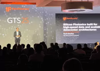
Silicon photonics took center stage as GF showcased measured results of 200 Gbps per wavelength transmission using micro-ring resonators fabricated on its photonics platform. These devices, which function as photonic transistors, have doubled bandwidth performance in less than two years—moving from 35 GHz to over 65 GHz—and now enable 200G transmission per channel. Dr. Letavic also previewed the RAMZI (Ring-Assisted Mach-Zehnder Interferometer) device, which breaks the traditional trade-off between bandwidth and extinction ratio. With demonstrated bandwidths approaching 100 GHz, RAMZI devices open the door to 400 Gbps per wavelength, marking a critical step in data center re-architecture for AI workloads.
Beyond raw performance gains, GF is also applying AI-based design tools to accelerate innovation in photonics. Using physics-informed AI modeling, engineers are generating novel device geometries that dramatically shrink footprint—by as much as 10x reduction in area—while maintaining optical performance. These AI-generated structures are often unintuitive in design but can now be faithfully manufactured thanks to recent OPC upgrades in GF fabs. Letavic emphasized that such AI-assisted co-design of devices and systems will be critical for scaling photonic integration, enabling far faster cycles of innovation than traditional trial-and-error approaches.
GF also highlighted work on multiplexing/demultiplexing structures for stacking 4, 8, or 16 wavelengths on the same waveguide, as well as investigations into new electro-optical materials. Combining these with advanced packaging techniques gives GF a roadmap to extend performance well beyond 400 Gbps.
Turning to quantum computing, Dr. Letavic described how GF’s 22FDX platform is proving to be a strong foundation for quantum-enabling technologies. The platform supports quantum dot arrays with both top- and bottom-gate control, allowing tunable coupling of quantum states. Measured results have demonstrated quantum blockade behavior, clear evidence of single-electron spin qubits in silicon, and high-performance analog readout circuits. The presence of precision analog within the same CMOS platform makes 22FDX well-suited for hybrid quantum-classical systems. “What was once thought to be far in the future is now being demonstrated in silicon,” Letavic noted, emphasizing that fundamental quantum building blocks can be implemented on a commercial FD-SOI platform.
GF also underscored the role of advanced packaging as a unifying technology across its platforms. Its SLIT and SLATE initiatives support both homogeneous and heterogeneous wafer bonding, enabling integration of CMOS logic, RF, photonics, GaN, and novel memory in new system form factors. Demonstrations included RF switches stacked to reduce area by 40%, microLEDs bonded onto CMOS drivers to create on-chip light sources, and integrated inductors and capacitors enabling complete on-die power regulators. For high-speed data center links, GF presented results showing how discrete heterojunction bipolar transistors (HBTs) can be integrated through advanced packaging with FD-SOI logic, delivering bandwidth gains and 30% lower power dissipation in optical communication chains. These heterogeneous integration schemes provide system designers new options to balance performance, cost, and footprint.
Other highlights included progress on GaN-on-Silicon power devices, with demonstrated 100V structures for efficient data center power regulation, and advances in ReRAM memory, where GF has achieved predictable conduction models that lay the groundwork for widespread embedded memory adoption.
- GF demonstrated 200 Gbps per wavelength silicon photonics, with a path to 400 Gbps using RAMZI devices.
- AI-assisted design has reduced photonic device footprints by 10x and accelerated design cycles.
- The 22FDX platform supports quantum dot arrays, quantum blockade measurements, and spin-based qubit evidence in silicon.
- Advanced packaging initiatives SLIT and SLATE enable heterogeneous integration of CMOS, RF, photonics, GaN, and microLEDs.
- GF Labs runs about 50 active programs, with 35–40% involving direct customer collaboration.
“Our approach at GF Labs is to prove every innovation in silicon or material with measured results. That’s how we make the bold decisions that steer the industry,” said Dr. Ted Letavic.


🌐 Analysis: GlobalFoundries is positioning itself at the center of three critical technology transitions. Silicon photonics is moving rapidly toward 400 Gbps per wavelength, making it indispensable for hyperscale AI data centers. By incorporating AI-driven design, GF is also signaling that innovation cycles in photonics can accelerate beyond the pace of traditional EDA tools. On the quantum front, 22FDX evidence of qubits points to mainstream CMOS playing a role in hybrid architectures, an approach also being tested by Intel and IBM. Meanwhile, GF’s heterogeneous packaging roadmap puts it in direct competition with TSMC’s CoWoS and Intel’s Foveros, but its focus on system-level integration gives it a differentiated path.
🌐 We’re tracking the latest developments in networking silicon. Follow our ongoing coverage at: https://convergedigest.com/category/semiconductors/