• Home
  • Events Calendar
  • Blueprint Guidelines
  • Privacy Policy
  • Subscribe to Daily Newsletter
  • NextGenInfra.io
No Result
View All Result
Converge Digest
Monday, April 13, 2026
  • Home
  • Events Calendar
  • Blueprint Guidelines
  • Privacy Policy
  • Subscribe to Daily Newsletter
  • NextGenInfra.io
No Result
View All Result
Converge Digest
No Result
View All Result

Home » GlobalFoundries Eyes $575M Advanced Packaging Center in New York

GlobalFoundries Eyes $575M Advanced Packaging Center in New York

January 17, 2025
in Optical, Semiconductors
A A

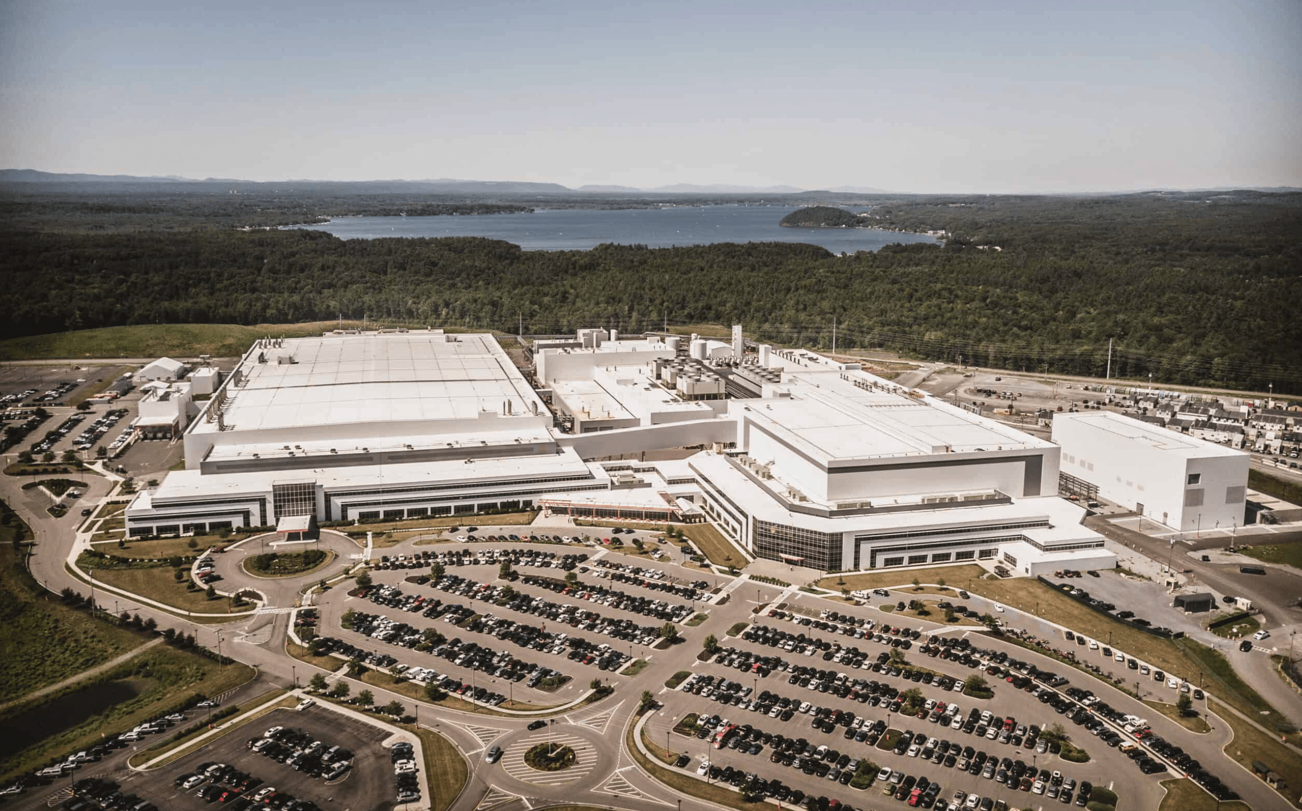
GlobalFoundries plans to establish the New York Advanced Packaging and Photonics Center at its Malta, New York, manufacturing facility. This first-of-its-kind center, supported by investments from New York State and the U.S. Department of Commerce, will focus on advanced packaging and testing for U.S.-made semiconductors used in critical industries such as AI, automotive, aerospace, defense, and communications. The initiative addresses the growing demand for silicon photonics and 3D/heterogeneously integrated (HI) chips, aiming to create a secure, end-to-end domestic semiconductor supply chain.

The center will deliver advanced packaging, bump, assembly, and testing capabilities for GF’s differentiated silicon photonics platform, which integrates optical and electrical components on a single chip. It will also provide turnkey packaging and testing for chips used in national security applications under GF’s Trusted Foundry accreditation, ensuring that sensitive devices remain entirely within the U.S. production pipeline. Additionally, it will support advanced packaging processes for 3D and HI chips using GF’s leading platforms, including 12LP+ and 22FDX®. These capabilities aim to position GF as a leader in semiconductor innovation and support geodiversity in supply chains for global customers.

With an expected investment of $575 million and an additional $186 million dedicated to research and development over the next decade, the center is projected to create approximately 100 new jobs at GF’s Malta facility, which already employs 2,500 people. The U.S. Department of Commerce will contribute up to $75 million in direct funding, supplemented by $20 million from New York State. This investment builds on the state’s prior $550 million support for GF under the Green CHIPS program.

• Key Features of the New York Advanced Packaging and Photonics Center:

• Silicon Photonics Platform: Advanced packaging and testing to combine optical and electrical components for enhanced power efficiency and performance.

• Trusted Foundry Accreditation: Secure production for aerospace and defense applications, ensuring chips remain in the U.S. throughout manufacturing.

• 3D/HI Chip Capabilities: Wafer-to-wafer bonding and assembly for leading GF platforms, such as 12LP+ and 22FDX®.

• Investment Breakdown: $575M for development and $186M for R&D over 10+ years.

“We’re proud to partner at the state and federal level on this new center, which is a direct response to our customers asking for more geodiversity in their supply chains and additional support with advanced packaging solutions for GF silicon photonics, Trusted, and 3D/HI offerings,” said Dr. Thomas Caulfield, President and CEO of GF.

Tags: GlobalFoundries
ShareTweetShare
Previous Post

Nokia and Ericsson Call for Urgent Action to Drive Innovation in Europe

Next Post

Corning, Edwards Vacuum, and Infinera Secure CHIPS Act Funding

Jim Carroll

Jim Carroll

Editor and Publisher, Converge! Network Digest, Optical Networks Daily - Covering the full stack of network convergence from Silicon Valley

Related Posts

GlobalFoundries acquires Tagore Technology’s GaN IP
Optical

GlobalFoundries Acquires InfiniLink for Silicon-Photonics Expertise

November 25, 2025
Semiconductor Industry Association projects rapid expansion in U.S. capacity
Semiconductors

GlobalFoundries and Silicon Labs Expand Partnership

October 30, 2025
GlobalFoundries Labs: Silicon Photonics, Quantum Silicon, Advanced Packaging
All

GlobalFoundries Labs: Silicon Photonics, Quantum Silicon, Advanced Packaging

August 28, 2025
GlobalFoundries Labs: Silicon Photonics, Quantum Silicon, Advanced Packaging
Video

Video: Silicon Photonics at an Inflection Point

August 28, 2025
GTS25: GlobalFoundries Doubles Down on Silicon Photonics
Semiconductors

GTS25: GlobalFoundries Doubles Down on Silicon Photonics

August 28, 2025
Semiconductor Industry Association projects rapid expansion in U.S. capacity
Semiconductors

GlobalFoundries Partners with Singapore’s A*STAR of Packaging R&D

May 20, 2025
Next Post
CHIPS for America allocates $3 billion for National Advanced Packaging

Corning, Edwards Vacuum, and Infinera Secure CHIPS Act Funding

Categories

  • 5G / 6G / Wi-Fi
  • AI Infrastructure
  • All
  • Automotive Networking
  • Blueprints
  • Clouds and Carriers
  • Data Centers
  • Enterprise
  • Explainer
  • Feature
  • Financials
  • Last Mile / Middle Mile
  • Legal / Regulatory
  • Optical
  • Quantum
  • Research
  • Security
  • Semiconductors
  • Space
  • Start-ups
  • Subsea
  • Sustainability
  • Video
  • Webinars

Archives

Tags

5G All AT&T Australia AWS Blueprint columns BroadbandWireless Broadcom China Ciena Cisco Data Centers Dell'Oro Ericsson FCC Financial Financials Huawei Infinera Intel Japan Juniper Last Mile Last Mille LTE Mergers and Acquisitions Mobile NFV Nokia Optical Packet Systems PacketVoice People Regulatory Satellite SDN Service Providers Silicon Silicon Valley StandardsWatch Storage TTP UK Verizon Wi-Fi
Converge Digest

A private dossier for networking and telecoms

Follow Us

  • Home
  • Events Calendar
  • Blueprint Guidelines
  • Privacy Policy
  • Subscribe to Daily Newsletter
  • NextGenInfra.io

© 2025 Converge Digest - A private dossier for networking and telecoms.

No Result
View All Result
  • Home
  • Events Calendar
  • Blueprint Guidelines
  • Privacy Policy
  • Subscribe to Daily Newsletter
  • NextGenInfra.io

© 2025 Converge Digest - A private dossier for networking and telecoms.

This website uses cookies. By continuing to use this website you are giving consent to cookies being used. Visit our Privacy and Cookie Policy.
Go to mobile version