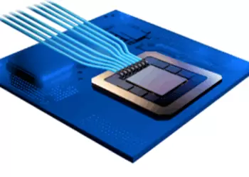
AI clusters are hitting a wall with copper cabling, and Avicena CEO Bardia Pezeshki believes microLEDs are the way through. At this week’s IEEE Hot Interconnects online conference, he revealed record-setting results showing microLED interconnects operating at under 0.3 pJ/bit while scaling to hundreds of channels—performance that could redefine scale-up networks inside data centers.
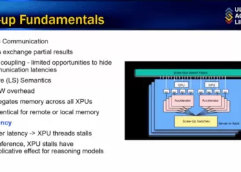
Pezeshki noted that today’s GPU clusters rely on thousands of short copper cables limited to one meter. With each GPU requiring 16 Tbps of connectivity, Nvidia estimates a potential $6 billion market for scale-up interconnects if costs fall to around $0.10 per Gbps. Silicon photonics and co-packaged optics have faced challenges with fiber alignment, laser reliability, and thermal stability. MicroLEDs, by contrast, avoid threshold currents, mode noise, isolators, and polarization issues. They operate reliably at high temperatures and leverage manufacturing advances from the display industry.
Avicena’s results include demonstration of 11.2 Gb/s per lane with error rates as low as 10⁻¹³, energy efficiency around 0.2–0.3 pJ/bit, and arrays of hundreds of LEDs transmitting up to 800 Gb/s in parallel. High-yield fabrication has been achieved, with negligible crosstalk between channels and redundancy options to tolerate device failures. Accelerated life tests at 4× nominal current density showed stable operation over thousands of hours. The company sees applications not only in scale-up GPU clusters but also in memory disaggregation with HBM and eventual co-packaged optics.
• GPU scale-up interconnect market estimated at $6B
• Targets: <5 pJ/bit, >1 Tbps/mm shoreline density, 10m reach, 10 FIT reliability
• Demonstrated: 0.2–0.3 pJ/bit with TSMC detectors, BER <10⁻¹³
• Parallel microLED arrays: 288 channels, ~800 Gb/s transmission
• Reliability: year-long life tests at 4× current density
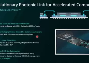
• Applications: active optical cables, CPO scale-up, memory disaggregation with HBM
“Large arrays of microLEDs can provide massive bandwidth at record-low energy. We believe this is a very exciting approach for short-reach, high-bandwidth communication in AI clusters and memory systems,” Pezeshki said.


🌐 Analysis: Avicena’s CEO underscored the technical foundation that differentiates microLED interconnects from silicon photonics. By eliminating lasers and using parallelism at scale, microLEDs offer unmatched energy efficiency and manufacturability. Early prototypes have already hit sub-pJ/bit levels—figures that undercut both copper and photonics. For data centers, this positions microLEDs as a candidate for near-term active optical cables and, longer term, co-packaged GPU-to-GPU and GPU-to-HBM links. Founded in 2019 in Sunnyvale, Avicena is moving quickly to commercialize its research, leveraging TSMC for detector integration and aiming to bring first products to market within two years.
🌐 We’re tracking the latest developments in networking silicon. Follow our ongoing coverage at: https://convergedigest.com/category/semiconductors/