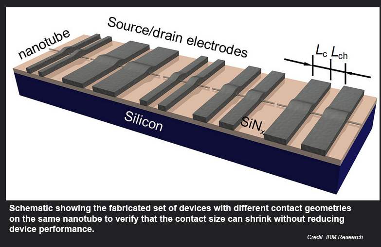
IBM researchers have demonstrated announced a new transistor contact approach that could accelerate the use carbon nanotubes as a replacement for silicon.
Previously, IBM shown that carbon nanotube transistors can operate as excellent switches at channel dimensions of less than ten nanometers – less than half the size of today’s leading silicon technology. IBM’s new contact approach overcomes the other major hurdle in incorporating carbon nanotubes into semiconductor devices, which could result in smaller chips with greater performance and lower power consumption.

The breakthrough required the invention of a metallurgical process akin to microscopic welding that chemically binds the metal atoms to the carbon atoms at the ends of nanotubes. IBM said this “end-bonded contact scheme” allows the contacts to be shrunken down to below 10 nanometers without deteriorating performance of the carbon nanotube devices.
“These chip innovations are necessary to meet the emerging demands of cloud computing, Internet of Things and Big Data systems,” said Dario Gil, vice president of Science & Technology at IBM Research. “As silicon technology nears its physical limits, new materials, devices and circuit architectures must be ready to deliver the advanced technologies that will be required by the Cognitive Computing era. This breakthrough shows that computer chips made of carbon nanotubes will be able to power systems of the future sooner than the industry expected.”
http://www-03.ibm.com/press/us/en/pressrelease/47767.wss
IBM Achieves 7nm Test Chips in Siilcon Germanium

IBM Research has produced the first 7nm (nanometer) node test chips with functioning transistors. The milestone was achieved using Silicon Germanium (SiGe) channel transistors and Extreme Ultraviolet (EUV) lithography integration at multiple levels. Current generation microprocessors are generally implemented in silicon using 22nm or 14nm technology. IBM partnered with GLOBALFOUNDRIES and Samsung at SUNY Polytechnic Institute’s Colleges of…
IBM’s Silicon Nanophotonics Integrates 25G Tranceivers in 90nm CMOS

IBM has integrated multiple optical components alongside electrical circuits using 90nm semiconductor process technology.
Essentially, IBM has successfully added a variety of silicon nanophotonics components, such as wavelength division multiplexers (WDM), modulators, and detectors, alongside CMOS electrical circuitry using a conventional semiconductor foundry.
IBM’s CMOS nanophotonics used transceivers exceeding 25 Gbps per channel. IBM said its integration is capable of feeding a number of parallel optical data streams into a single fiber by utilizing compact on-chip wavelength-division multiplexing devices. The ability to multiplex large data streams at high data rates will allow future scaling of optical communications capable of delivering terabytes of data between distant parts of computer systems.
http://www-03.ibm.com/press/us/en/pressrelease/39641.wss
- In October 2012, IBM announced a breakthrough in building a semiconductor using carbon nanotubes instead of silicon. IBM researchers created a device consisting of more than ten thousand working transistors made of nano-sized tubes of carbon. Standard semiconductor processes were used to fabricate the device. IBM has previously demonstrated that carbon nanotube transistors can operate as excellent switches at molecular dimensions of less than ten nanometers – less than half the size of the leading silicon technology.