• Home
  • Events Calendar
  • Blueprint Guidelines
  • Privacy Policy
  • Subscribe to Daily Newsletter
  • NextGenInfra.io
No Result
View All Result
Converge Digest
Saturday, April 11, 2026
  • Home
  • Events Calendar
  • Blueprint Guidelines
  • Privacy Policy
  • Subscribe to Daily Newsletter
  • NextGenInfra.io
No Result
View All Result
Converge Digest
No Result
View All Result

Home » IBM Develops Co-Packaged Optics Integrating PWG

IBM Develops Co-Packaged Optics Integrating PWG

December 10, 2024
in Optical
A A

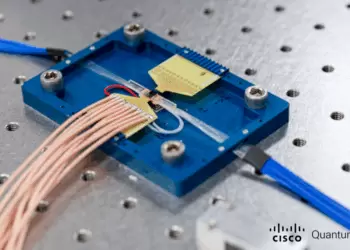
IBM has introduced a new co-packaged optics (CPO) technology that integrates polymer optical waveguides (PWG) to replace electrical interconnects inside data centers. Designed to support the growing demands of generative AI, this innovation enables chip-to-chip and board-to-board communication using optical signals, offering significant improvements in bandwidth density, energy efficiency, and scalability. The prototype achieves an 80-fold increase in bandwidth compared to traditional electrical pathways while drastically reducing energy consumption.

The system leverages 50-micrometer-pitch PWGs, which are adiabatically coupled to silicon photonics waveguides using standard assembly processes. These optical connections transmit terabits of data per second across distances ranging from a few centimeters to hundreds of meters, eliminating the bottlenecks of copper wiring. IBM’s CPO module supports six times the beachfront density (optical fibers at a chip’s edge) compared to existing solutions. The company has also demonstrated scalability to 18-micrometer-pitch PWGs, enabling up to 128 optical channels on a single module.

Key Points:

• Bandwidth Increase: Offers up to 80x the bandwidth of electrical interconnects, transmitting data at 10 Tbps/mm.

• Energy Efficiency: Reduces power consumption by over five times, saving energy equivalent to powering 5,000 U.S. homes annually during AI training.

• Faster AI Model Training: Reduces training time for Large Language Models from three months to three weeks.

• Extended Reach: Enables interconnect lengths of hundreds of meters, surpassing electrical wire limitations.

• Durability: Components pass JEDEC reliability tests, including operation in -40°C to 125°C environments and high-humidity conditions.

Researchers developed and tested the modules at IBM’s facilities in Albany, New York, and Bromont, Quebec, part of the Northeast Semiconductor Corridor. These efforts highlight IBM’s focus on advancing semiconductor manufacturing and packaging technologies to address emerging computing challenges.

“As generative AI demands more energy and processing power, the data center must evolve—and co-packaged optics can make these data centers future-proof,” said Dario Gil, SVP and Director of Research at IBM. “This innovation enables chips to communicate optically, paving the way for faster, more efficient AI systems.”

Tags: CPOIBM
ShareTweetShare
Previous Post

Nokia Adds SONiC Support to Data Center Switching Portfolio

Next Post

Micron Secures $6.165 Billion in CHIPS Act Funding

Jim Carroll

Jim Carroll

Editor and Publisher, Converge! Network Digest, Optical Networks Daily - Covering the full stack of network convergence from Silicon Valley

Related Posts

IBM and Cisco Aim for Networked, Fault-Tolerant Quantum by Early 2030s
Quantum

IBM and Cisco Aim for Networked, Fault-Tolerant Quantum by Early 2030s

November 20, 2025
Applied Materials and GlobalFoundries Launch Waveguide Facility 
Optical

Tower Extends Wafer-Bonding Tech to SiPho + SiGe for Data-Center Optics

November 12, 2025
IBM Doubles Quantum R&D Speed With 300 mm Fab
Quantum

IBM Doubles Quantum R&D Speed With 300 mm Fab

November 12, 2025
Airtel and IBM Partner to Expand AI-Ready Cloud Infrastructure
All

Airtel and IBM Partner to Expand AI-Ready Cloud Infrastructure

October 23, 2025
Broadcom Unveils 102.4 Tbps “Davisson” CPO Switch for AI Clusters
All

Broadcom Unveils 102.4 Tbps “Davisson” CPO Switch for AI Clusters

October 8, 2025
Video: Inside Broadcom’s 102.4 Tbps “Davisson” Switch
Video

Video: Inside Broadcom’s 102.4 Tbps “Davisson” Switch

October 8, 2025
Next Post
CHIPS for America allocates $3 billion for National Advanced Packaging

Micron Secures $6.165 Billion in CHIPS Act Funding

Categories

  • 5G / 6G / Wi-Fi
  • AI Infrastructure
  • All
  • Automotive Networking
  • Blueprints
  • Clouds and Carriers
  • Data Centers
  • Enterprise
  • Explainer
  • Feature
  • Financials
  • Last Mile / Middle Mile
  • Legal / Regulatory
  • Optical
  • Quantum
  • Research
  • Security
  • Semiconductors
  • Space
  • Start-ups
  • Subsea
  • Sustainability
  • Video
  • Webinars

Archives

Tags

5G All AT&T Australia AWS Blueprint columns BroadbandWireless Broadcom China Ciena Cisco Data Centers Dell'Oro Ericsson FCC Financial Financials Huawei Infinera Intel Japan Juniper Last Mile Last Mille LTE Mergers and Acquisitions Mobile NFV Nokia Optical Packet Systems PacketVoice People Regulatory Satellite SDN Service Providers Silicon Silicon Valley StandardsWatch Storage TTP UK Verizon Wi-Fi
Converge Digest

A private dossier for networking and telecoms

Follow Us

  • Home
  • Events Calendar
  • Blueprint Guidelines
  • Privacy Policy
  • Subscribe to Daily Newsletter
  • NextGenInfra.io

© 2025 Converge Digest - A private dossier for networking and telecoms.

No Result
View All Result
  • Home
  • Events Calendar
  • Blueprint Guidelines
  • Privacy Policy
  • Subscribe to Daily Newsletter
  • NextGenInfra.io

© 2025 Converge Digest - A private dossier for networking and telecoms.

This website uses cookies. By continuing to use this website you are giving consent to cookies being used. Visit our Privacy and Cookie Policy.
Go to mobile version