Intel Labs has established an academically-oriented Integrated Photonics Research Center with a mission to accelerate optical input/output (I/O) technology innovation in performance scaling and integration with a specific focus on photonics technology and devices, CMOS circuits and link architecture, and package integration and fiber coupling.
The Intel Research Center for Integrated Photonics for Data Center Interconnects will bring together leading university researchers to accelerate optical I/O technology innovation in performance scaling and integration. The research vision is to explore a technology scaling path that satisfies energy efficiency and bandwidth performance requirements for the next decade and beyond.

“At Intel Labs, we’re strong believers that no one organization can successfully turn all the requisite innovations into research reality. By collaborating with some of the top scientific minds from across the United States, Intel is opening the doors for the advancement of integrated photonics for the next generation of compute interconnect. We look forward to working closely with these researchers to explore how we can overcome impending performance barriers,” stated James Jaussi, senior principal engineer and director of the PHY Research Lab in Intel Labs.
The researchers participating in the Research Center include:
- John Bowers, University of California, Santa Barbara
Project: Heterogeneously Integrated Quantum Dot Lasers on Silicon.
Description: The UCSB team will investigate issues with integrating indium arsenide (InAs) quantum dot lasers with conventional silicon photonics. The goal of this project is to characterize expected performance and design parameters of single frequency and multiwavelength sources. - Pavan Kumar Hanumolu, University of Illinois, Urbana-Champaign
Project: Low-power optical transceivers enabled by duo-binary signaling and baud-rate clock recovery.
Description: This project will develop ultra-low-power, high-sensitivity optical receivers using novel trans-impedance amplifiers and baud-rate clock and data recovery architectures. The prototype optical transceivers will be implemented in a 22 nm CMOS process to demonstrate very high jitter tolerance and excellent energy efficiency. - Arka Majumdar, University of Washington
Project: Nonvolatile reconfigurable optical switching network for high-bandwidth data communication.
Description: The UW team will work on low-loss, nonvolatile electrically reconfigurable silicon photonic switches using emerging chalcogenide phase change materials. Unlike existing tunable mechanisms, the developed switch will hold its state, allowing zero static power consumption. - Samuel Palermo, Texas A&M University
Project: Sub-150fJ/b optical transceivers for data center interconnects.
Description: This project will develop energy-efficient optical transceiver circuits for a massively parallel, high-density and high-capacity photonic interconnect system. The goal is to improve energy efficiency by employing dynamic voltage frequency scaling in the transceivers, low-swing voltage-mode drivers, ultra-sensitive optical receivers with tight photodetector integration, and low-power optical device tuning loops. - Alan Wang, Oregon State University
Project: 0.5V silicon microring modulators driven by high-mobility transparent conductive oxide.
Description: This project seeks to develop a low driving voltage, high bandwidth silicon microring resonator modulator (MRM) through heterogeneous integration between the silicon MOS capacitor with high-mobility Ti:In2O3 The device promises to overcome the energy efficiency bottleneck of the optical transmitter and can be co-packaged in future optical I/O systems. - Ming Wu, University of California, Berkeley
Project: Wafer-scale optical packaging of silicon photonics.
Description: The UC Berkeley team will develop integrated waveguide lenses that have potential to enable non-contact optical packaging of fiber arrays with low loss and high tolerances. - S.J. Ben Yoo, University of California, Davis
Project: Athermal and power-efficient scalable high-capacity silicon-photonic transceivers.
Description: The UC Davis team will develop extremely power-efficient athermal silicon-photonic modulator and resonant photodetector photonic integrated circuits scaling to 40 Tb/s capacity at 150 fJ/b energy efficiency and 16 Tb/s/mm I/O density. To achieve this, the team will also develop a new 3D packaging technology for vertical integration of photonic and electronic integrated circuits with 10,000 pad-per-square-mm interconnect-pad-density.
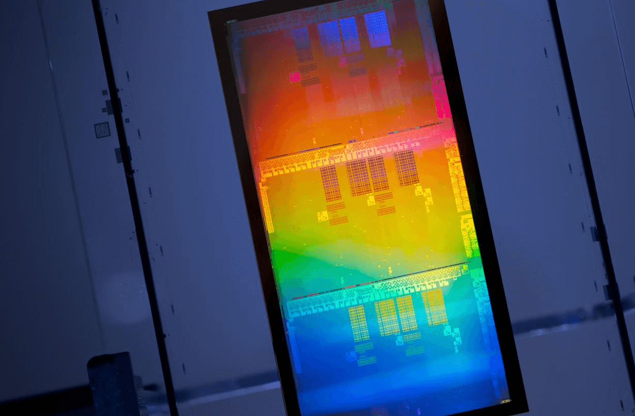
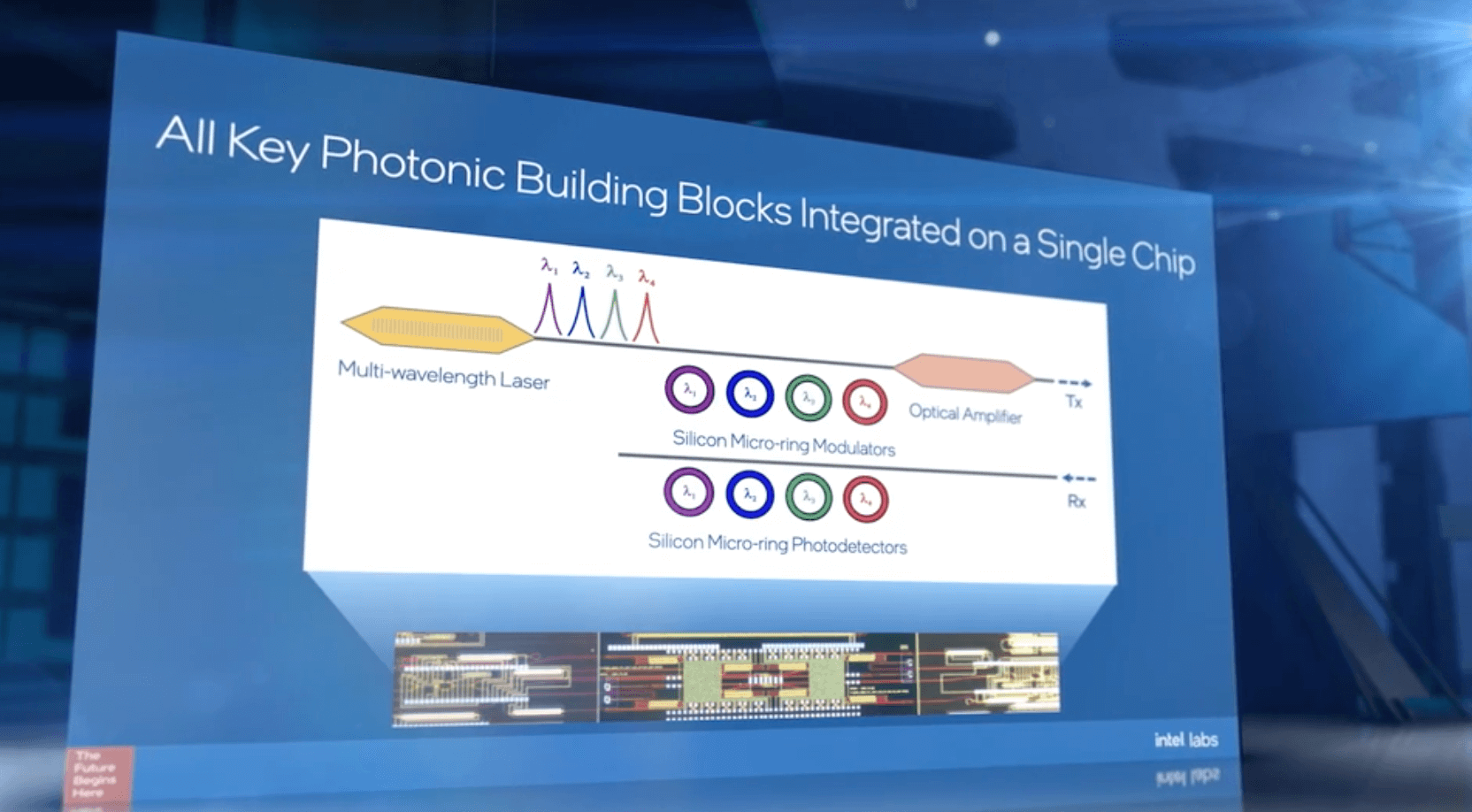
Intel shows micro-ring modulators, all-silicon photodetectors, multi-lambda lasers
Intel showcased a number of advancements in the field of optical interconnects, advancing its long-term ambition to bring optical I/O directly into silicon packages. During a virtual Intel Labs day presentatio, the company demonstrated advances in key technology building blocks, including with light generation, amplification, detection, modulation, complementary metal-oxide semiconductor (CMOS) interface circuits and package integration.

Key technology building blocks showcased:
- Micro-ring modulators: Conventional silicon modulators take up too much area and are costly to place on IC packages. By developing micro-ring modulators, Intel has miniaturized the modulator by a factor of more than 1,000, thereby eliminating a key barrier to integrating silicon photonics onto a compute package.
- All-silicon photodetector: For decades, the industry has believed silicon has virtually no light detection capability in the 1.3-1.6um wavelength range. Intel showcased research that proves otherwise. Lower cost is one of the main benefits of this breakthrough.
- Integrated semiconductor optical amplifier: As the focus turns to reducing total power consumption, integrated semiconductor optical amplifiers are an indispensable technology, made possible with the same material used for the integrated laser.
- Integrated multi-wavelength lasers: Using a technique called wavelength division multiplexing, separate wavelengths can be used from the same laser to convey more data in the same beam of light. This enables additional data to be transmitted over a single fiber, increasing bandwidth density.
- Integration: By tightly integrating silicon photonics and CMOS silicon through advanced packaging techniques, we can gain three benefits: lower power, higher bandwidth and reduced pin count. Intel is the only company that has demonstrated integrated multi-wavelength lasers and semiconductor optical amplifiers, all-silicon photodetectors, and micro-ring modulators on a single technology platform tightly integrated with CMOS silicon. This research breakthrough paves the path for scaling integrated photonics.
Intel said these advancements will enable future architectures that are more disaggregated, with multiple functional blocks such as compute, memory, accelerators and peripherals spread throughout the entire network and interconnected via optical and software in high-speed and low-latency links.
“We are approaching an I/O power wall and an I/O bandwidth gap that will dramatically hinder performance scaling. The rapid progress Intel is making in integrated photonics will enable the industry to fully re-imagine data center networks and architectures that are connected by light. We have now demonstrated all of the critical optical technology building blocks on one silicon platform, tightly integrated with CMOS silicon. Our research on tightly integrating photonics with CMOS silicon can systematically eliminate barriers across cost, power and size constraints to bring the transformative power of optical interconnects to server packages,” stated James Jaussi, senior principal engineer and director of PHY Lab, Intel Labs.
Without such advancements, Intel warns the industry will soon reach the practical limits of electrical I/O performance – what it calls an “I/O power wall”.