Intel Labs has demonstrated an eight-wavelength distributed feedback (DFB) laser array that is fully integrated on a silicon wafer. The laser array, which is built on Intel’s commercial 300-millimeter silicon photonics manufacturing process, delivers output power uniformity of +/- 0.25 decibel (dB) and wavelength spacing uniformity of ±6.5% that exceed industry specifications.

Intel Labs says this advancement will enable the production of the optical source with the required performance for future high-volume applications, such as co-packaged optics and optical compute interconnect. The fabrication of the eight-wavelength DFB laser array employed the same process which is used to manufacture production optical transceivers in volume. Specifically, Intel used advanced lithography to define the waveguide gratings in silicon prior to the III-V wafer bonding process. This technique resulted in better wavelength uniformity compared to conventional semiconductor lasers manufactured in 3-inch or 4-inch III-V wafer fabs. In addition, due to the tight integration of the lasers, the array also maintains its channel spacing when the ambient temperature is changed.

In addition, many aspects of the eight-wavelength integrated laser array technology are being implemented by Intel’s Silicon Photonics Products Division as part of a future optical compute interconnect chiplet product. The forthcoming product will offer power-efficient, high-performance multi-terabits per second interconnect between compute resources including CPUs, GPUs and memory. The integrated laser array is a critical element to achieve a compact and cost-effective solution that supports high-volume manufacturing and deployment.
“This new research demonstrates that it’s possible to achieve well-matched output power with uniform and densely spaced wavelengths. Most importantly, this can be done using existing manufacturing and process controls in Intel’s fabs, thereby ensuring a clear path to volume production of the next-generation co-packaged optics and optical compute interconnect at scale,” states Haisheng Rong, senior principal engineer at Intel Labs.
https://www.intel.com/content/www/us/en/research/overview.html
Intel establishes Integrated Photonics Research Center

Intel Labs has established an academically-oriented Integrated Photonics Research Center with a mission to accelerate optical input/output (I/O) technology innovation in performance scaling and integration with a specific focus on photonics technology and devices, CMOS circuits and link architecture, and package integration and fiber coupling.The Intel Research Center for Integrated Photonics for Data Center Interconnects will bring together leading…
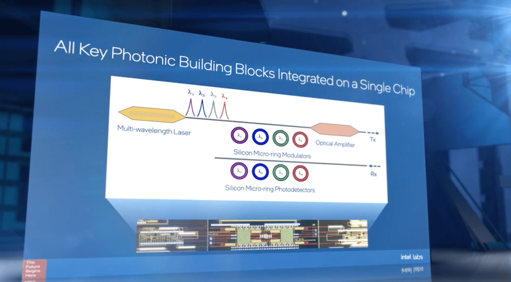
Intel shows micro-ring modulators, all-silicon photodetectors, multi-lambda lasers

Intel showcased a number of advancements in the field of optical interconnects, advancing its long-term ambition to bring optical I/O directly into silicon packages. During a virtual Intel Labs day presentatio, the company demonstrated advances in key technology building blocks, including with light generation, amplification, detection, modulation, complementary metal-oxide semiconductor (CMOS) interface circuits and package integration. Key…