• Home
  • Events Calendar
  • Blueprint Guidelines
  • Privacy Policy
  • Subscribe to Daily Newsletter
  • NextGenInfra.io
No Result
View All Result
Converge Digest
Sunday, April 12, 2026
  • Home
  • Events Calendar
  • Blueprint Guidelines
  • Privacy Policy
  • Subscribe to Daily Newsletter
  • NextGenInfra.io
No Result
View All Result
Converge Digest
No Result
View All Result

Home » Intel to upgrade its New Mexico fab for 3D semiconductor packaging

Intel to upgrade its New Mexico fab for 3D semiconductor packaging

May 3, 2021
in Semiconductors
A A

Intel announced plans to $3.5 billion to equip its New Mexico operations for the manufacturing of advanced semiconductor packaging technologies, including Foveros, its 3D packaging technology.

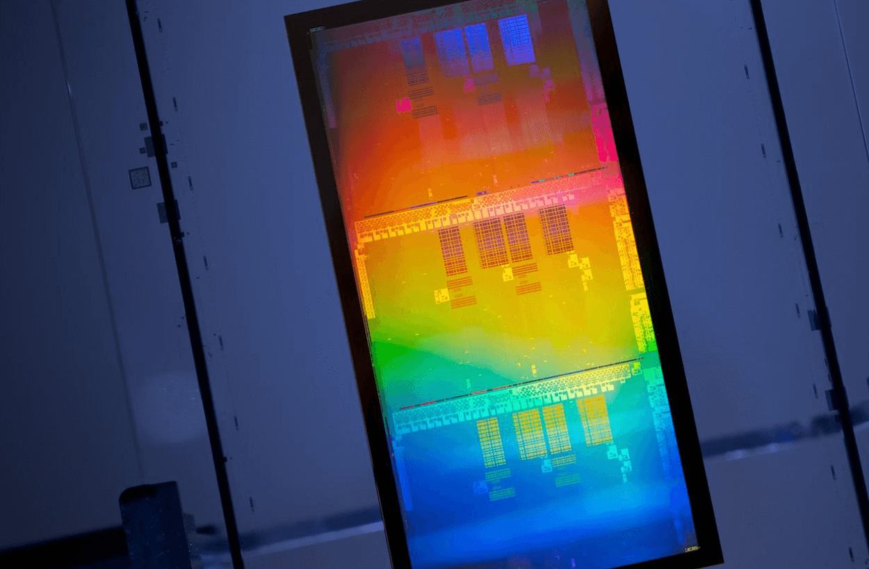
Foveros advanced 3D packaging technology enables Intel to build processors with compute tiles stacked vertically, rather than side-by-side, providing greater performance in a smaller footprint. It also allows Intel to mix and match compute tiles to optimize for cost and power efficiency. 

“A key differentiator for our IDM 2.0 strategy is our unquestioned leadership in advanced packaging, which allows us to mix and match compute tiles to deliver the best products. We’re seeing tremendous interest in these capabilities from the industry, especially following the introduction of our new Intel Foundry Services. We’re proud to have invested in New Mexico for more than 40 years and we see our Rio Rancho campus continuing to play a critical role in Intel’s global manufacturing network in our new era of IDM 2.0,” stated Keyvan Esfarjani, Intel senior vice president and general manager of Manufacturing and Operations.

  • In 2018, Intel first demonstrated a new 3D packaging technology, called “Foveros,” which for the first time brings 3D stacking to logic-on-logic integration.
    Foveros will allow products to be broken up into smaller “chiplets,” where I/O, SRAM and power delivery circuits can be fabricated in a base die and high-performance logic chiplets are stacked on top. 


U.S. DoD backs Intel for semiconductor packaging tech

Sunday, October 04, 2020  Intel, Military, Silicon  

The U.S. Department of Defense awarded a contract to Intel to enable the U.S. government to access Intel’s state-of-the-art semiconductor packaging capabilities in Arizona and Oregon.The project, which is supported by the DoD’s State-of-the-Art Heterogeneous Integration Prototype (SHIP) program,  is executed by the Naval Surface Warfare Center, Crane Division, and administered by the National Security Technology Accelerator.The second phase…

READ MORE

Tags: IntelSilicon
ShareTweetShare
Previous Post

Cologix acquire data center in Silicon Valley

Next Post

SpaceX completes 26th Starlink launch mission, its 10th for 2021

Staff

Staff

Related Posts

Intel Q3 2025: AI Partnerships, Foundry Momentum, and U.S. Backing 
All

Intel Q3 2025: AI Partnerships, Foundry Momentum, and U.S. Backing 

October 23, 2025
Intel Ramps 18A Production at Fab 52
Semiconductors

Intel Ramps 18A Production at Fab 52

October 9, 2025
Intel Foundry Services forms USMAG Alliance
Semiconductors

NVIDIA and Intel Forge $5B Partnership to Build Data Center and PC Chips

September 18, 2025
Intel’s Q3 data center revenue dropped 27% yoy
Financials

Intel Names New Data Center, Client, and Foundry Leaders

September 8, 2025
Intel cites progress with U.S. fabs
Semiconductors

U.S. Takes 9.9% Stake in Intel with $8.9B Equity Investment

August 22, 2025
Intel breaks ground on its new fab in Ohio
Financials

Intel Posts Flat Revenue for Q2, Restructuring and Impairments

July 24, 2025
Next Post
Windstream Enterprise Achieves MEF 3.0 SD-WAN Certification

Windstream Enterprise Achieves MEF 3.0 SD-WAN Certification

Please login to join discussion

Categories

  • 5G / 6G / Wi-Fi
  • AI Infrastructure
  • All
  • Automotive Networking
  • Blueprints
  • Clouds and Carriers
  • Data Centers
  • Enterprise
  • Explainer
  • Feature
  • Financials
  • Last Mile / Middle Mile
  • Legal / Regulatory
  • Optical
  • Quantum
  • Research
  • Security
  • Semiconductors
  • Space
  • Start-ups
  • Subsea
  • Sustainability
  • Video
  • Webinars

Archives

Tags

5G All AT&T Australia AWS Blueprint columns BroadbandWireless Broadcom China Ciena Cisco Data Centers Dell'Oro Ericsson FCC Financial Financials Huawei Infinera Intel Japan Juniper Last Mile Last Mille LTE Mergers and Acquisitions Mobile NFV Nokia Optical Packet Systems PacketVoice People Regulatory Satellite SDN Service Providers Silicon Silicon Valley StandardsWatch Storage TTP UK Verizon Wi-Fi
Converge Digest

A private dossier for networking and telecoms

Follow Us

  • Home
  • Events Calendar
  • Blueprint Guidelines
  • Privacy Policy
  • Subscribe to Daily Newsletter
  • NextGenInfra.io

© 2025 Converge Digest - A private dossier for networking and telecoms.

No Result
View All Result
  • Home
  • Events Calendar
  • Blueprint Guidelines
  • Privacy Policy
  • Subscribe to Daily Newsletter
  • NextGenInfra.io

© 2025 Converge Digest - A private dossier for networking and telecoms.

This website uses cookies. By continuing to use this website you are giving consent to cookies being used. Visit our Privacy and Cookie Policy.
Go to mobile version