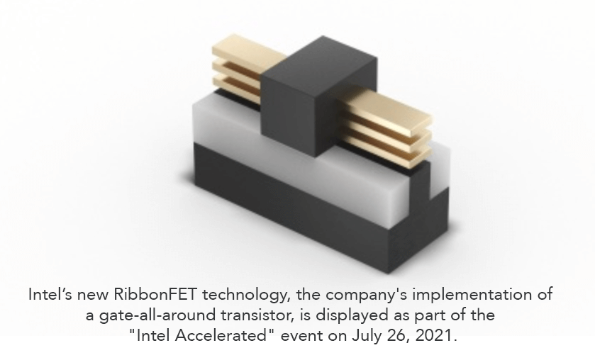
Intel unveiled RibbonFET, its first new transistor architecture in more than a decade, and PowerVia, a new backside power delivery method.

In a webcast presentation highlighting its process and packaging technology roadmaps through 2025, Intel vowed a swift adoption of next-generation extreme ultraviolet lithography (EUV), referred to as High Numerical Aperture (High NA) EUV. The company said it is on-track to received the first High NA EUV production tool in the industry.
Intel’s roadmap, with new node names, includes:
- Intel 7 delivers an approximately 10% to 15% performance-per-watt increase versus Intel 10nm SuperFin, based on FinFET transistor optimizations. Intel 7 will be featured in products such as Alder Lake for client in 2021 and Sapphire Rapids for the data center, which is expected to be in production in the first quarter of 2022.
- Intel 4 fully embraces EUV lithography to print incredibly small features using ultra-short wavelength light. With an approximately 20% performance-per-watt increase, along with area improvements, Intel 4 will be ready for production in the second half of 2022 for products shipping in 2023, including Meteor Lake for client and Granite Rapids for the data center.

- Intel 3 leverages further FinFET optimizations and increased EUV to deliver an approximately 18% performance-per-watt increase over Intel 4, along with additional area improvements. Intel 3 will be ready to begin manufacturing products in the second half of 2023.
- Intel 20A ushers in the angstrom era with two breakthrough technologies, RibbonFET and PowerVia. RibbonFET, Intel’s implementation of a gate-all-around transistor, will be the company’s first new transistor architecture since it pioneered FinFET in 2011. The technology delivers faster transistor switching speeds while achieving the same drive current as multiple fins in a smaller footprint. PowerVia is Intel’s unique industry-first implementation of backside power delivery, optimizing signal transmission by eliminating the need for power routing on the front side of the wafer. Intel 20A is expected to ramp in 2024. The company is also excited about the opportunity to partner with Qualcomm using its Intel 20A process technology.
- 2025 and Beyond: Beyond Intel 20A, Intel 18A is already in development for early 2025 with refinements to RibbonFET that will deliver another major jump in transistor performance. Intel is also working to define, build and deploy next-generation High NA EUV, and expects to receive the first production tool in the industry. Intel is partnering closely with ASML to assure the success of this industry breakthrough beyond the current generation of EUV.
“Intel has a long history of foundational process innovations that have propelled the industry forward by leaps and bounds,” said Dr. Ann Kelleher, senior vice president and general manager of Technology Development. “We led the transition to strained silicon at 90nm, to high-k metal gates at 45nm and to FinFET at 22nm. Intel 20A will be another watershed moment in process technology with two groundbreaking innovations: RibbonFET and PowerVia.”
Regarding its packaging innovations, Intel provided the following updates:
- Sapphire Rapids will be the first Intel Xeon data center product to ship in volume with EMIB (embedded multi-die interconnect bridge). It will also be the first dual-reticle-sized device in the industry, delivering nearly the same performance as a monolithic design. Beyond Sapphire Rapids, the next generation of EMIB will move from a 55-micron bump pitch to 45 microns.
- Foveros leverages wafer-level packaging capabilities to provide a first-of-its-kind 3D stacking solution. Meteor Lake will be the second-generation implementation of Foveros in a client product and features a bump pitch of 36 microns, tiles spanning multiple technology nodes and a thermal design power range from 5 to 125W.
- Foveros Omni ushers in the next generation of Foveros technology by providing unbounded flexibility with performance 3D stacking technology for die-to-die interconnect and modular designs. Foveros Omni allows die disaggregation, mixing multiple top die tiles with multiple base tiles across mixed fab nodes and is expected to be ready for volume manufacturing in 2023.
- Foveros Direct moves to direct copper-to-copper bonding for low-resistance interconnects and blurs the boundary between where the wafer ends and where the package begins. Foveros Direct enables sub-10-micron bump pitches, providing an order of magnitude increase in the interconnect density for 3D stacking, opening new concepts for functional die partitioning that were previously unachievable. Foveros Direct is complementary to Foveros Omni and is also expected to be ready in 2023.