• Home
  • Events Calendar
  • Blueprint Guidelines
  • Privacy Policy
  • Subscribe to Daily Newsletter
  • NextGenInfra.io
No Result
View All Result
Converge Digest
Sunday, April 12, 2026
  • Home
  • Events Calendar
  • Blueprint Guidelines
  • Privacy Policy
  • Subscribe to Daily Newsletter
  • NextGenInfra.io
No Result
View All Result
Converge Digest
No Result
View All Result

Home » Keysight Launches Automation Software to Streamline Photonic Circuit Design

Keysight Launches Automation Software to Streamline Photonic Circuit Design

March 19, 2025
in Optical
A A

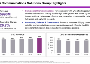
Keysight Technologies has introduced Photonic Designer, a new photonic design automation (PDA) software aimed at improving accuracy, streamlining workflows, and ensuring compliance for photonic integrated circuit (PIC) engineers. As part of Keysight’s Advanced Design System (ADS) tool suite, Photonic Designer addresses common industry challenges such as fragmented toolchains and simulation inconsistencies by providing an end-to-end design, simulation, and validation environment.

The software integrates real-world measurement data into its simulation engine to enhance model precision and compliance verification. Engineers can now validate photonic circuit designs against industry modulation standards before fabrication, customize models to match foundry process conditions, and ensure compatibility with photonic foundry PDKs. Photonic Designer is built to optimize both optical-only and electro-optical-electrical workflows, helping reduce costly design iterations and accelerate time-to-market for PICs.

CompoundTek, a leading photonics foundry service provider, will also offer a verified PDK for Keysight’s Photonic Designer, enabling engineers to design silicon photonic circuits with foundry-ready components. Keysight highlights this new platform as a unified solution that reduces unnecessary tool-switching, simplifies compliance, and delivers high-fidelity results from initial concept to full manufacturing handoff.

• Keysight launches Photonic Designer as part of the ADS suite, streamlining photonic circuit design and simulation.

• Provides physics-based simulations with real-world measurement data integration for enhanced design accuracy.

• Enables pre-fabrication verification against modulation standards and foundry-specific PDK alignment.

• Supports combined optical and electro-optical-electrical workflows in a single design environment.

• CompoundTek releases foundry-verified silicon photonics PDK for Photonic Designer users.

“Photonic Designer provides a single, unified platform that integrates physics-based simulations, PDK customization, and compliance verification, ensuring high-fidelity results from concept to manufacturing,” said Nilesh Kamdar, EDA Design & Verification General Manager at Keysight.


Tags: Keysight
ShareTweetShare
Previous Post

Geoffrey Starks to Step Down as FCC Commissioner

Next Post

Cirion Taps Windstream Wholesale for Backbone Connectivity

Jim Carroll

Jim Carroll

Editor and Publisher, Converge! Network Digest, Optical Networks Daily - Covering the full stack of network convergence from Silicon Valley

Related Posts

Keysight Closes FY25 With $1.42B in Q4 Revenue, Order Rebound
Financials

Keysight Closes FY25 With $1.42B in Q4 Revenue, Order Rebound

November 24, 2025
Spirent and Nokia show 800G interoperability
All

Keysight Completes £1.16 Billion Acquisition of Spirent Communications

October 16, 2025
Rapidus Taps Keysight to Sharpen 2nm PDK and Boost Yield at IIM-1
Semiconductors

Rapidus Taps Keysight to Sharpen 2nm PDK and Boost Yield at IIM-1

August 26, 2025
#OFC25 Video: Next-Gen 224G & 448G/Lane Electrical Connectivity
Video

#OFC25 Video: Breaking Records: 448G/Lane Demo with PAM-4

April 7, 2025
Keysight Launches KAI Architecture for Data Center Design, Validation, and Deployment
All

Keysight Launches KAI Architecture for Data Center Design, Validation, and Deployment

April 3, 2025
Keysight, NTT, and Lumentum Hit 448 Gbps per Lane Optical Milestone
Optical

Keysight, NTT, and Lumentum Hit 448 Gbps per Lane Optical Milestone

April 2, 2025
Next Post
Windstream Wholesale builds 864-count buried dark fiber route in Eastern U.S.

Cirion Taps Windstream Wholesale for Backbone Connectivity

Categories

  • 5G / 6G / Wi-Fi
  • AI Infrastructure
  • All
  • Automotive Networking
  • Blueprints
  • Clouds and Carriers
  • Data Centers
  • Enterprise
  • Explainer
  • Feature
  • Financials
  • Last Mile / Middle Mile
  • Legal / Regulatory
  • Optical
  • Quantum
  • Research
  • Security
  • Semiconductors
  • Space
  • Start-ups
  • Subsea
  • Sustainability
  • Video
  • Webinars

Archives

Tags

5G All AT&T Australia AWS Blueprint columns BroadbandWireless Broadcom China Ciena Cisco Data Centers Dell'Oro Ericsson FCC Financial Financials Huawei Infinera Intel Japan Juniper Last Mile Last Mille LTE Mergers and Acquisitions Mobile NFV Nokia Optical Packet Systems PacketVoice People Regulatory Satellite SDN Service Providers Silicon Silicon Valley StandardsWatch Storage TTP UK Verizon Wi-Fi
Converge Digest

A private dossier for networking and telecoms

Follow Us

  • Home
  • Events Calendar
  • Blueprint Guidelines
  • Privacy Policy
  • Subscribe to Daily Newsletter
  • NextGenInfra.io

© 2025 Converge Digest - A private dossier for networking and telecoms.

No Result
View All Result
  • Home
  • Events Calendar
  • Blueprint Guidelines
  • Privacy Policy
  • Subscribe to Daily Newsletter
  • NextGenInfra.io

© 2025 Converge Digest - A private dossier for networking and telecoms.

This website uses cookies. By continuing to use this website you are giving consent to cookies being used. Visit our Privacy and Cookie Policy.
Go to mobile version