• Home
  • Events Calendar
  • Blueprint Guidelines
  • Privacy Policy
  • Subscribe to Daily Newsletter
  • NextGenInfra.io
No Result
View All Result
Converge Digest
Friday, April 10, 2026
  • Home
  • Events Calendar
  • Blueprint Guidelines
  • Privacy Policy
  • Subscribe to Daily Newsletter
  • NextGenInfra.io
No Result
View All Result
Converge Digest
No Result
View All Result

Home » Kyoto Semiconductor intros Two-Wavelength Photodiode

Kyoto Semiconductor intros Two-Wavelength Photodiode

May 26, 2020
in All
A A

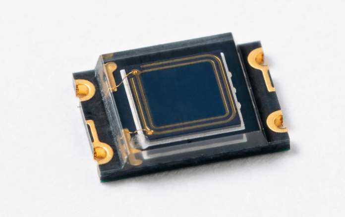
Kyoto Semiconductor Co. introduced a Two-Wavelength Photodiode with photosensitivity for a wide range of wavelengths, from 400 to 1,700 nm, arrayed along the same light axis. The device is capable of being surface-mounted, with silicon and indium-gallium-arsenide photodiodes. Samples will be available from August 31, 2020.

Applications could include spectroscopic analysis, enabling the identification of objects and their characteristics by reflecting light off those objects and measuring the degrees of transmission and reflection.

https://www.kyosemi.co.jp/en/lp/kpmc29

Tags: Blueprint columnsJapanKyotoSilicon
ShareTweetShare
Previous Post

A1 Telecom Austria picks Netcracker for OSS

Next Post

Samsung Electronics intros stand-alone security chip for mobiles

Staff

Staff

Related Posts

Nokia Integrates MantaRay SON into NTT DOCOMO’s Multi-Vendor 5G Network
5G / 6G / Wi-Fi

Nokia Integrates MantaRay SON into NTT DOCOMO’s Multi-Vendor 5G Network

November 24, 2025
NTT Showcases Optical–Quantum and Expands IOWN Strategy
Optical

NTT Showcases Optical–Quantum and Expands IOWN Strategy

November 18, 2025
NVIDIA to Invest $1B in Nokia, Partnership for AI-RAN and Data Center Networking
5G / 6G / Wi-Fi

Nokia Wins 5G RAN Contract from SoftBank in Japan

November 5, 2025
SoftBank Expands All-Optical Nationwide with Cisco 400G
Clouds and Carriers

SoftBank Expands All-Optical Nationwide with Cisco 400G

October 23, 2025
STACK Expands with ¥39.7B Financing for 36MW Tokyo Campus
Data Centers

STACK Expands with ¥39.7B Financing for 36MW Tokyo Campus

October 22, 2025
Fujitsu Taps NVLink Fusion for MONAKA CPUs + NVIDIA GPUs for Industrial AI
AI Infrastructure

Fujitsu Taps NVLink Fusion for MONAKA CPUs + NVIDIA GPUs for Industrial AI

October 3, 2025
Next Post
Xilinx spins 20-nm, radiation-tolerant, space-grade FPGAs

Xilinx spins 20-nm, radiation-tolerant, space-grade FPGAs

Please login to join discussion

Categories

  • 5G / 6G / Wi-Fi
  • AI Infrastructure
  • All
  • Automotive Networking
  • Blueprints
  • Clouds and Carriers
  • Data Centers
  • Enterprise
  • Explainer
  • Feature
  • Financials
  • Last Mile / Middle Mile
  • Legal / Regulatory
  • Optical
  • Quantum
  • Research
  • Security
  • Semiconductors
  • Space
  • Start-ups
  • Subsea
  • Sustainability
  • Video
  • Webinars

Archives

Tags

5G All AT&T Australia AWS Blueprint columns BroadbandWireless Broadcom China Ciena Cisco Data Centers Dell'Oro Ericsson FCC Financial Financials Huawei Infinera Intel Japan Juniper Last Mile Last Mille LTE Mergers and Acquisitions Mobile NFV Nokia Optical Packet Systems PacketVoice People Regulatory Satellite SDN Service Providers Silicon Silicon Valley StandardsWatch Storage TTP UK Verizon Wi-Fi
Converge Digest

A private dossier for networking and telecoms

Follow Us

  • Home
  • Events Calendar
  • Blueprint Guidelines
  • Privacy Policy
  • Subscribe to Daily Newsletter
  • NextGenInfra.io

© 2025 Converge Digest - A private dossier for networking and telecoms.

No Result
View All Result
  • Home
  • Events Calendar
  • Blueprint Guidelines
  • Privacy Policy
  • Subscribe to Daily Newsletter
  • NextGenInfra.io

© 2025 Converge Digest - A private dossier for networking and telecoms.

This website uses cookies. By continuing to use this website you are giving consent to cookies being used. Visit our Privacy and Cookie Policy.
Go to mobile version