At last week’s Optica Photonic-Enabled Cloud Computing (PECC) Summit, Darius Bunandar, Founder and Chief Scientist at Lightmatter, described how 3D photonic integration will redefine the architecture of AI and high-performance computing systems. Bunandar said the limits of copper interconnects and 2D packaging are forcing a new generation of optical architectures designed for density, bandwidth, and energy efficiency.

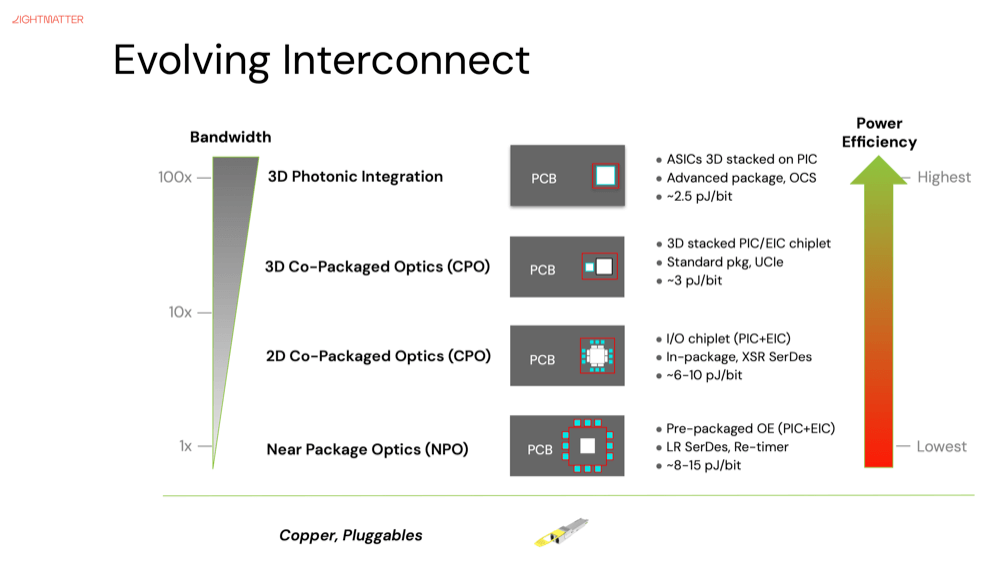
“The fundamental problem,” Bunandar said, “is that communication still happens on the chip perimeter — there’s simply not enough shoreline to scale bandwidth.” Lightmatter’s solution is a 3D co-packaged photonic architecturethat stacks compute and optical layers to bring photonics directly into the heart of the system. The company’s Passage™ L- and M-Series platforms combine electronic integrated circuits (EICs) and photonic integrated circuits (PICs) using advanced packaging and UCIe chiplet interfaces, achieving energy efficiency down to ~2.5 pJ/bitin its most advanced 3D designs.
Key highlights from the presentation:
• 3D Photonic Integration – ASICs are vertically stacked on photonic interposers for unprecedented density and bandwidth. The progression from Near-Package Optics (NPO, ~8–15 pJ/bit) to full 3D CPO (~2.5 pJ/bit) represents more than an order-of-magnitude gain in efficiency.
• Microring modulators (MRMs) – Serving as the “heart of the engine,” Lightmatter’s MRMs are ultra-compact, high-speed, and inherently wavelength-division-multiplexing (WDM) friendly. Each microring handles one wavelength channel, allowing dense wavelength multiplexing on a single fiber.
• Bidirectional 16-wavelength link – Lightmatter demonstrated a 16λ bidirectional DWDM link delivering 800 Gb/s per fiber over 1 km single-mode fiber with BER < 1E-9 without FEC, operating with <5 pJ/bit energy efficiency and excellent thermal stability.
• Thermal robustness – MRMs maintained performance across temperature cycling from 25°C to 105°C and back, and under aggressive 800°C/s transients using an on-die heater.
• External WDM laser (Guide™) – Provides up to 16 wavelengths on a 200 GHz grid, optimized for microring transmitter architectures.
• Rack-scale modeling – Simulation of Lightmatter’s Passage architecture shows 32T optical scale-up bandwidth per GPU—reducing model training time by up to 17× versus electrical-only scale-up clusters.
Bunandar said that 3D CPO architectures will become the natural successor to today’s 2D co-packaged optics, overcoming both heat and density barriers in next-generation AI systems. “We’re collapsing the distance between compute and photonics,” he said. “This isn’t just about faster links—it’s about flattening the AI cluster so models train faster and at lower energy.”
Lightmatter, founded by photonics researchers from MIT, is developing integrated optical computing and networking platforms that merge high-speed photonics with semiconductor scaling. Its Passage, Envise, and Guide product families target AI data centers, next-generation supercomputers, and optical interconnect fabrics.


www.lightmatter.co