• Home
  • Events Calendar
  • Blueprint Guidelines
  • Privacy Policy
  • Subscribe to Daily Newsletter
  • NextGenInfra.io
No Result
View All Result
Converge Digest
Saturday, April 18, 2026
  • Home
  • Events Calendar
  • Blueprint Guidelines
  • Privacy Policy
  • Subscribe to Daily Newsletter
  • NextGenInfra.io
No Result
View All Result
Converge Digest
No Result
View All Result

Home » MIT’s novel photolithography targets thin mirrors and silicon wafers

MIT’s novel photolithography targets thin mirrors and silicon wafers

April 20, 2022
in Optical, Semiconductors
A A

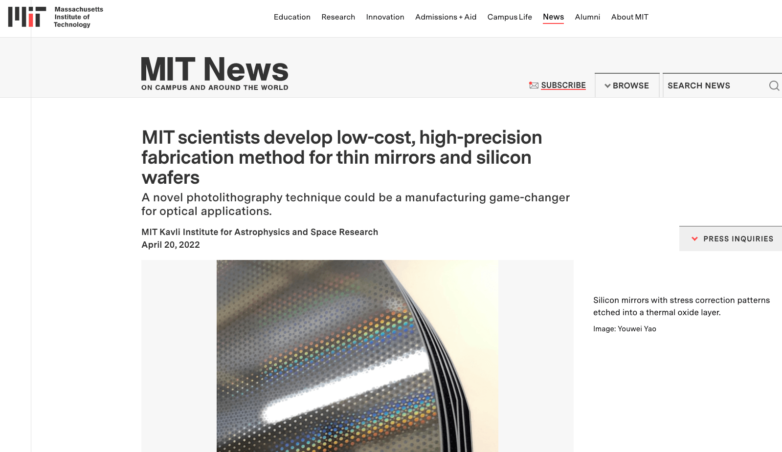
Researchers at MIT have developed a novel photolithography technique that could significantly improve the fabrication of thin mirrors and silicon wafers.

The new approach to reshaping thin plate materials enables precise and complex shapes typically used for high-level, complex systems, like deformable mirrors or wafer-flattening processes during semiconductor manufacturing. By printing stress patterns lithographically to deform optical or semiconductor surfaces, the researchers believe future production will be more precise, scalable, and cheap.

The research is published in the April 20 issue of Optica.

https://news.mit.edu/2022/mit-scientists-develop-low-cost-high-precision-fabrication-method-thin-mirrors-and-silicon-0420

Tags: AcademiaMITOpticalSilicon
ShareTweetShare
Previous Post

Lightwave Logic cites hybrid polymer-silicon photonics innovation

Next Post

Comcast tests Lumenisity’s hollowcore fiber

Staff

Staff

Related Posts

CBRE Group acquires Direct Line Global for data center infrastructure
Optical

NYU Researchers Discover Hybrid Liquid-Crystal Material 

November 8, 2025
Microsoft Inks 5-Year, Multi-Billion Deal with KT to Drive AI in Korea
Optical

Open RAN xHaul and IPoDWDM Solutions Take Center Stage

February 27, 2025
Montage Technology Samples PCIe 6.x/CXL 3.x Retimer Chips
Data Centers

Montage Technology Samples PCIe 6.x/CXL 3.x Retimer Chips

January 22, 2025
Ribbon Communications Secures $385 million credit facility
Optical

Ribbon Completes DWDM Deployment for Bharti Airtel

October 27, 2024
Tech Update video: Ayar Labs’ Optical I/O Chiplets
Optical

ECOC24 video: What’s Next for Optical DSPs? 1.6T and Beyond

September 24, 2024
Jefferson Lab and ESnet Stream Physics Data Coast-to-Coast at 100 Gbps
All

Jefferson Lab and ESnet Stream Physics Data Coast-to-Coast at 100 Gbps

September 24, 2024
Next Post
Comcast tests Lumenisity’s hollowcore fiber

Comcast tests Lumenisity's hollowcore fiber

Please login to join discussion

Categories

  • 5G / 6G / Wi-Fi
  • AI Infrastructure
  • All
  • Automotive Networking
  • Blueprints
  • Clouds and Carriers
  • Data Centers
  • Enterprise
  • Explainer
  • Feature
  • Financials
  • Last Mile / Middle Mile
  • Legal / Regulatory
  • Optical
  • Quantum
  • Research
  • Security
  • Semiconductors
  • Space
  • Start-ups
  • Subsea
  • Sustainability
  • Video
  • Webinars

Archives

Tags

5G All AT&T Australia AWS Blueprint columns BroadbandWireless Broadcom China Ciena Cisco Data Centers Dell'Oro Ericsson FCC Financial Financials Huawei Infinera Intel Japan Juniper Last Mile Last Mille LTE Mergers and Acquisitions Mobile NFV Nokia Optical Packet Systems PacketVoice People Regulatory Satellite SDN Service Providers Silicon Silicon Valley StandardsWatch Storage TTP UK Verizon Wi-Fi
Converge Digest

A private dossier for networking and telecoms

Follow Us

  • Home
  • Events Calendar
  • Blueprint Guidelines
  • Privacy Policy
  • Subscribe to Daily Newsletter
  • NextGenInfra.io

© 2025 Converge Digest - A private dossier for networking and telecoms.

No Result
View All Result
  • Home
  • Events Calendar
  • Blueprint Guidelines
  • Privacy Policy
  • Subscribe to Daily Newsletter
  • NextGenInfra.io

© 2025 Converge Digest - A private dossier for networking and telecoms.

This website uses cookies. By continuing to use this website you are giving consent to cookies being used. Visit our Privacy and Cookie Policy.
Go to mobile version