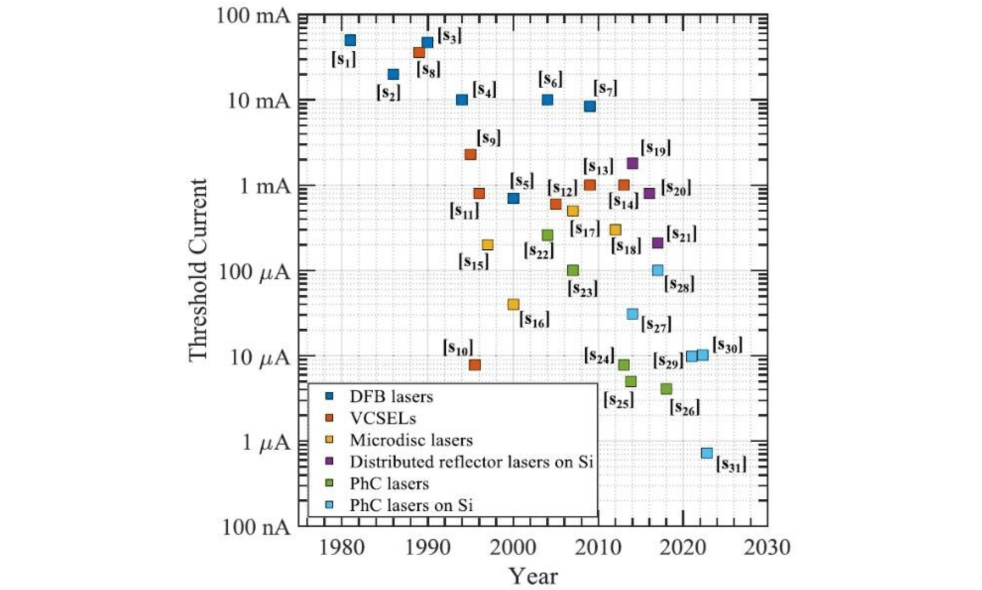
A new generation of semiconductor nanolasers is set to power advances in on-chip optical communications and neuromorphic computing, according to a new paper from researchers at the Technical University of Denmark. Published in IEEE Journal of Selected Topics in Quantum Electronics, the study highlights recent breakthroughs that dramatically reduce energy consumption while enabling deep subwavelength light confinement — both critical for next-generation optical systems.
Since their invention in 1962, semiconductor lasers have underpinned modern telecommunications, sensing, and imaging. But traditional designs are now being challenged by the growing need for compact, faster, and more efficient photonic components. The research team, led by Prof. Jesper Mørk, reports that miniaturizing laser cavities to the nanoscale offers significant performance gains and opens new directions in laser physics.
The paper outlines three key innovations:
- Photonic crystal nanolasers that use periodic structures to trap light in ultra-small cavities, with threshold currents as low as 730 nA.
- Deep subwavelength cavities that beat traditional diffraction limits without relying on lossy metals.
- Semiconductor Fano lasers that exploit interference effects to produce ultrashort optical pulses and enhanced spectral characteristics.
“Miniaturizing laser cavities to the nanoscale not only enables unprecedented energy efficiency but also challenges our understanding of fundamental laser physics,” the authors write.
Reference: Nanostructured Semiconductor Lasers, IEEE Journal of Selected Topics in Quantum Electronics, DOI: 10.1109/JSTQE.2024.3483900