At the recent OIF 448G Workshop in Santa Clara, Tad Hofmeister, Optical Hardware Engineer on Google’s Machine Learning Systems team, offered a deep dive into Google’s evolving AI infrastructure and made a compelling case for accelerating industry-wide support for 448Gbps electrical interfaces. Hofmeister, a long-time OIF contributor now focused on data center interconnects for AI workloads, outlined the demands of hyperscale AI clusters—both Google’s custom TPU-based systems and NVIDIA-based GPU clusters—and their growing reliance on high-speed, high-density connectivity to handle scale-up and scale-out traffic.
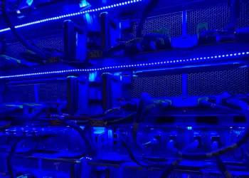
Hofmeister emphasized that while power and cost are always factors, the central motivation for 448G is simple: XPUs are running out of I/O escape. As Google’s Ironwood TPUs and NVIDIA’s Grace Blackwell GPUs push the limits of on-chip compute, the need to move more data between devices becomes critical. Hofmeister detailed both Google’s proprietary ICI-based TPU topology—which uses optical interconnects between cube-style clusters—and NVIDIA’s rack-contained NVLink GPU architectures, highlighting how both platforms demand massive bandwidth density and flexibility, with increasing adoption of co-packaged copper (CPC) to overcome signal integrity and density challenges.
He urged standards bodies to prioritize fast decision-making, suggesting the industry choose between PAM6 and PAM8 to avoid delays, and supported new front-panel connector MSAs tailored for 448G, even at the expense of backward compatibility. Hofmeister concluded by warning against designs that cannot be reliably serviced at scale and encouraged the community to adopt solutions that support flexibility, testability, and production viability.

• Google’s TPU-based AI clusters use a proprietary interconnect with optical circuit switching between racks, enabling scale-up to 9,216 TPUs per superpod.
• XPU trays must support both copper and optical interconnects via modular OSFPs for flexible deployment.
• The move to 448G is driven by package I/O limitations, not just performance or power savings.
• Google is skeptical that PAM4 will close at 448G and advocates for PAM6 or PAM8.
• Co-packaged copper is critical to bypass PCB limitations and achieve SerDes targets.
• Front-panel pluggables with improved connectors and possibly 12V power are needed to support up to 50W modules for high-performance optics.
• New connector MSAs should prioritize signal integrity over backward compatibility.
• Reliability, serviceability, and supply chain flexibility must be core design principles.
Tad Hofmeister, Optical Hardware Engineer, Google:
“448G isn’t just about speed—it’s about survival. We’re hitting the ceiling on how many SerDes we can escape from these XPUs. The path forward requires rethinking connector design, embracing co-packaged copper, and accepting that some legacy constraints must be broken to get where AI needs us to go.”
Want to be involved our video series? Contact info@nextgeninfra.io
https://ngi.fyi/oif448-google-tad