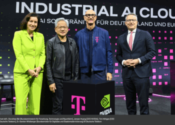
Speaking at the Photonic Enabled Cloud Computing (PECC) Summit, co-hosted by Optica and the Advanced Photonics Coalition at the HPE + Juniper Networks Aspiration Dome, Ashkan Seyedi, Senior Director at NVIDIA, presented a detailed look into how network architecture defines the scalability, performance, and economics of artificial intelligence infrastructure.
- AI inference revenue depends directly on moving data efficiently across GPUs.
- NVIDIA’s Ethernet-based AI networking delivers up to 35% higher performance than standard implementations.
- Spectrum-X and SuperNIC platforms reduce jitter, latency, and congestion across hyperscale clusters.
- Co-packaged optics (CPO) integration cuts power and improves system reliability.
- Balance between scale-up and scale-out bandwidth is essential to maintain power and thermal efficiency.
- NVIDIA’s AI factories now scale toward 500,000 GPUs per campus, drawing over 600 megawatts of compute power.
Networking as a Source of Revenue

Seyedi reframed networking as the true engine of AI revenue. “KV caches don’t make money when they sit still—they make money when they move,” he said. In NVIDIA’s large-scale inference deployments, the movement of model data between accelerators determines utilization and ultimately profitability.
He emphasized that AI networks are not merely plumbing for compute but are now tied directly to revenue generation and total cost of ownership. Every transfer of cache between GPUs represents a productive cycle, much like a financial transaction in motion.
Ethernet Tuned for AI
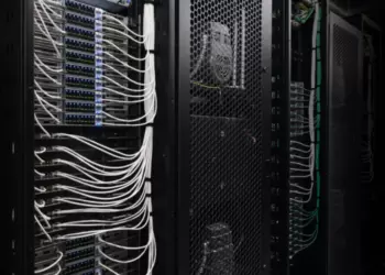
NVIDIA’s next-generation Ethernet architecture, derived from InfiniBand principles, has been deployed by Meta, Oracle, and xAI to support massive AI training clusters. These systems feature congestion control, traffic shaping, and flow isolation tailored to GPU workloads.
The company reports 30–35% better performance for multi-tenant AI workloads, with reduced jitter and improved latency consistency. Spectrum-X switches and SuperNICs work as a tightly integrated system to maintain deterministic performance across thousands of nodes.
“Just because you call it Ethernet doesn’t mean it behaves like Ethernet,” Seyedi said. “If it only works with one vendor’s NICs, switches, and software, that’s not really open.”
Balancing Scale-Up and Scale-Out
Seyedi discussed the need to maintain balance between scale-up and scale-out network bandwidths. GPUs must manage three interconnected fabrics—HBM on-package memory, NVLink for intra-node communication, and Ethernet or InfiniBand for cluster-scale communication.
“If your interconnect isn’t ten times lower in power and smaller in size, it’s going to be a deployment headache at AI scale,” he said. Even small inefficiencies multiply across hundreds of thousands of GPUs.
Co-Packaged Optics: From Concept to Production
To meet power and reliability targets at hyperscale, NVIDIA is deploying co-packaged optics across both InfiniBand and Ethernet lines. By placing optical engines adjacent to the switch ASIC, NVIDIA removes several electrical conversion steps, reducing loss, voltage regulation overhead, and failure points.
“The best component in your system is the one you don’t use,” Seyedi said, noting that CPO designs simplify thermal management while increasing bandwidth density. Each module integrates lasers, drivers, and photonics in a compact package to support multi-terabit connectivity per switch.

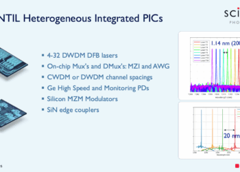
Advances in Photonics
Seyedi noted renewed industry confidence in microwave photonics and micro-ring modulators, technologies that had once been considered too unstable for large-scale deployment. “We made microrings cool again,” he joked.
He also addressed the growing interest in micro-LEDs for photonic interconnects but urged caution. “The LED might be perfect—zero picojoules per bit—but if you can’t connect it, it’s useless.” He reminded the audience that the connector and fiber ecosystem, built over decades of Telco standardization, remains the economic foundation of optical networking.
Design Realism and System Thinking
Seyedi cautioned against unrealistic assumptions in chip and package design. “You don’t put the kitchen at the front door,” he said, referring to impractical claims of placing I/O anywhere on a die. Practical layout constraints, thermal budgets, and manufacturability still govern system architecture.
He urged photonics and networking startups to evaluate innovation at the system level rather than in isolation. “Keep your eye on how the solution scales—thermally, electrically, and economically. That’s where innovation really counts.”