SK hynix plans to invest an estimated $3.87 billion to build a state-of-the-art advanced packaging fabrication and R&D facility for AI products in West Lafayette, Indiana.
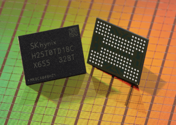
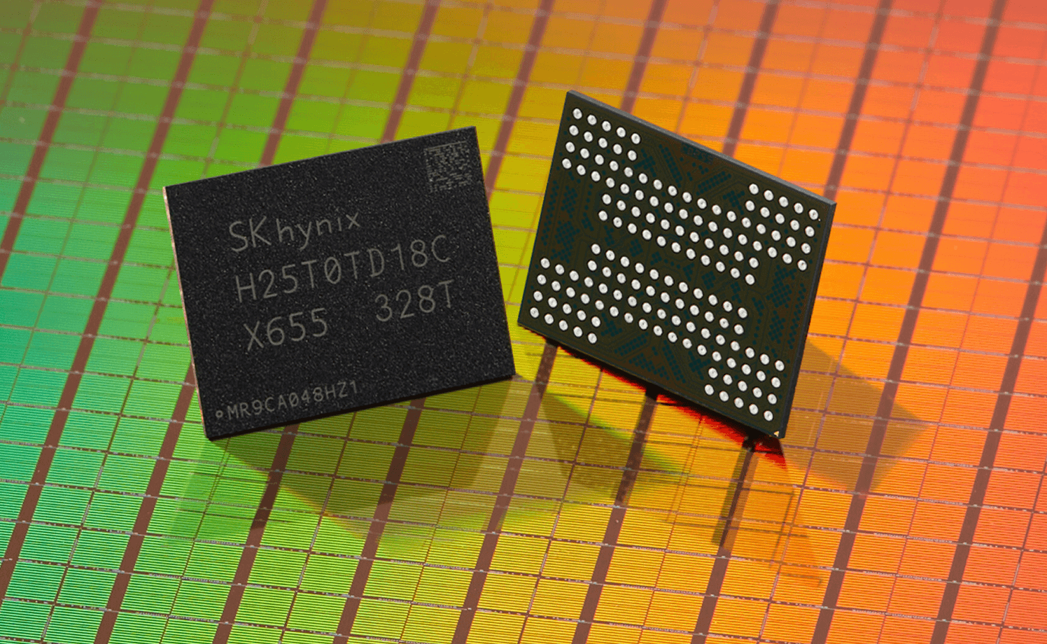
SK hynix is the world’s leading producer of High-Bandwidth Memory (HBM) chips. The new facility will be home to an advanced semiconductor production line that will mass-produce next-generation HBM, the highest-performing Dynamic Random Access Memory (DRAM) chips, which are the critical components of graphic processing units that train AI systems such as ChatGPT. The company plans to begin mass production in the second half of 2028, while the new facility will also develop future generations of chips and house an advanced packaging R&D line.
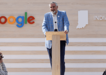
At the event, officials from each party including Governor of Indiana Eric Holcomb, Senator Todd Young, Director of the White House Office of Science and Technology Policy Arati Prabhakar, Assistant Secretary of Commerce Arun Venkataraman, Secretary of Commerce State of Indiana David Rosenberg, Purdue University President Mung Chiang, Chairman of Purdue Research Foundation Mitch Daniels, Mayor of city of West Lafayette Erin Easter, Ambassador of the Republic of Korea to the United States Hyundong Cho, Consul General of the Republic of Korea in Chicago Junghan Kim, SK vice chairman Jeong Joon Yu, SK hynix CEO Kwak Noh-Jung and SK hynix Head of Package & Test Choi Woojin, participated.
“SK hynix is the global pioneer and dominant market leader in memory chips for AI,” Purdue University President Mung Chiang said. “This transformational investment reflects our state and university’s tremendous strength in semiconductors, hardware AI, and hard tech corridor. It is also a monumental moment for completing the supply chain of digital economy in our country through chips advanced packaging. Located at Purdue Research Park, the largest facility of its kind at a U.S. university will grow and succeed through innovation.”
“We are excited to become the first in the industry to build a state-of-the-art advanced packaging facility for AI products in the United States that will help strengthen supply-chain resilience and develop a local semiconductor ecosystem,” said SK hynix CEO Kwak Noh-Jung. “With this new facility, we hope to advance our goal of providing AI memory chips with unmatched capabilities, serving the needs of our customers.”
SK hynix is collaborating with Purdue University, one of the leading research institutions in the U.S., on plans for future R&D projects. These projects include work on advanced packaging and heterogeneous integration with Purdue’s Birck Nanotechnology Center and other research institutes and industry partners. They also hope to collaborate on a project related to memory-centric solutions and architecture for the generative AI era, specifically system-level memory design and in/near-memory computing.
The company also plans to collaborate with Purdue University and Ivy Tech Community College to develop training programs and interdisciplinary degree curricula that will cultivate a high-tech workforce and build a reliable pipeline of new talent.
Separately, SK hynix will also proceed with Korean domestic investments as planned. The company has been working to prepare the site for the Yongin Semiconductor Cluster where it will invest 120 trillion won to build production facilities. The company plans to break ground on the first fab in March of 2025, with plans for completion in early 2027. It will also build a mini fab, a facility with equipment for 300mm wafer processing, to test semiconductor materials, components and equipment.