Synopsys and Juniper Networks are establishing a joint venture company focused on open silicon photonics for applications such as telecom, datacom, LiDAR, healthcare, HPC, AI, and optical computing.

The new company’s open silicon photonics platform will include integrated lasers, optical amplifiers, and a full suite of photonic components to form a complete solution that will be accessible through a Process Design Kit (PDK). The platform promises the lowest power consumption for high-performance Photonic Integrated Circuits (PICs).
The new company, which has not yet been named, will be jointly owned, with Synopsys holding the majority share. It is being formed, in part, from the carve-out of integrated silicon photonics assets from Juniper, which includes more than 200 patents on photonic device design and process integration.
While part of Juniper, the new company has closely collaborated with Tower Semiconductor to develop and qualify Tower Semiconductor’s PH18DA process technology to enable the industry’s first “laser-on-a-chip” open silicon photonics platform. To demonstrate capabilities of this platform and accelerate customer adoption of the technology, the new company has created 400G and 800G photonics reference designs with integrated lasers and expects first samples to be available in summer 2022.
A key challenge for silicon photonics has been the cost of adding discrete lasers, which includes the manufacturing as well as the assembly and alignment of those lasers onto the photonic chip. This becomes more important as the number of laser channels and the overall bandwidth increases. By processing the Indium Phosphide (InP) materials directly onto the silicon photonics wafer, the PH18DA platform reduces the cost and time of adding lasers, enabling volume scalability and improved power efficiency. In addition, monolithically integrated lasers on silicon wafers improves overall reliability and simplifies packaging. This “Laser-on-a-Chip” open silicon photonics platform will bring integrated photonics to a host of new applications and markets that were previously not thought possible. The first Multi-Project Wafer (MPW) is scheduled to be taped out in Q2 2022.
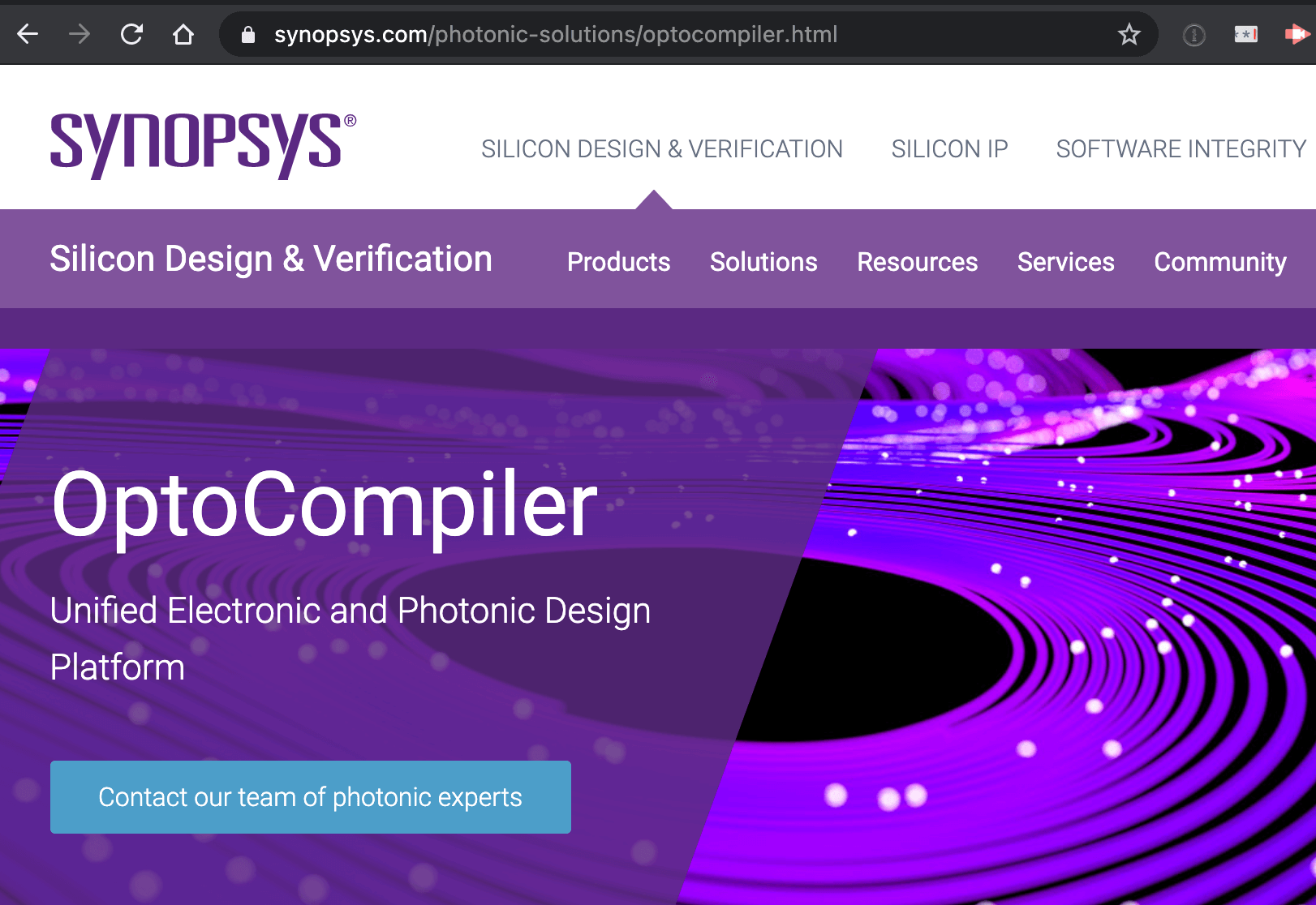
“Silicon photonics is a rapidly growing market that is transforming many industries and creating exciting opportunities for new applications in the future,” said Sassine Ghazi, president and chief operating officer at Synopsys. “The new company’s open silicon photonics platform, combined with Synopsys’ existing investment in a unified electronic photonic design automation solution consisting of OptoCompiler™, OptSim™, PrimeSim™, Photonic Device Compiler and IC Validator™ products, will help reshape the optical computing industry, enabling companies to cost-effectively shift to integrated lasers and significantly accelerate development of photonic IC designs.”
“This revolutionary technology will change the economics of how people are going to build photonic systems,” said Rami Rahim, CEO of Juniper Networks. “We have been strong supporters of integrated silicon photonics and we believe the new company will drive development of these systems by using an advanced open platform that will dramatically reduce costs and increase the performance and reliability of designs across multiple use cases. We are excited to continue to collaborate with the new company to enable a broad ecosystem to efficiently develop next-generation optical transceiver and co-packaged designs.”
“We have had a long history of successful collaboration with Juniper Networks on integrated photonics. The new company formed by Synopsys and Juniper will strengthen and accelerate the adoption of the silicon photonics platform,” said Russell Ellwanger, CEO of Tower Semiconductor. “Providing an open silicon photonics platform consisting of integrated lasers that has been qualified on Tower’s process will enable customers to create innovative products with the potential to transform the industry.”
Juniper picks Synopsys for developing photonics-enabled chips

Synopsys is supplying its OptoCompiler platform, including the OptSim and PrimeSim HSPICE simulation solutions, to Juniper Networks to accelerate the development of photonic-enabled chips for the next generation of optical communications.Juniper plans to use Synopsys solutions to design and optimize its hybrid silicon and InP optical platform.”Synopsys offers a unique, unified photonic and electronic design suite, which accelerates customer design…
Tower Semi and Juniper develop silicon photonics process
Tower Semiconductor and Juniper Networks announced a silicon photonics (SiPho) foundry-ready process with integrated III-V lasers, amplifiers modulators and detectors.
Potential applications include optical connectivity in datacenters and telecom networks, as well as AI, LiDAR and other sensors.
The new platform co-integrates III-V lasers, semiconductor optical amplifiers (SOA), electro-absorption modulators (EAM) and photodetectors with silicon photonics devices, all monolithically on a single chip. This enables smaller, higher-channel count and more power-efficient optical architectures and solutions. Foundry availability will enable a broad array of product developers to create highly integrated photonic integrated circuits (PICs) for diverse markets.

Process design kits (PDK) are expected to be available by year end and the first open multi-project wafer (MPW) run are expected to be offered early next year. First samples of full 400Gb/s and 800Gb/s PICs reference designs with integrated laser are expected to be available in the second quarter of 2022.
“Our mutual development work with Tower has been extraordinarily successful in qualifying this innovative silicon photonics technology in a high-volume manufacturing facility,” said Rami Rahim, CEO of Juniper Networks. “By offering this capability to the entire industry, Juniper offers the potential to radically reduce the cost of optics while lowering the barrier to entry for customers”.
“Our partnership with Juniper on silicon photonics is bringing a paradigm shift for product development across our industry,” said Russell Ellwanger, CEO of Tower Semiconductor. “It is now possible to mix the advantages of III-V semiconductors with high-volume silicon photonics manufacturing. Being the singular open market, integrated laser silicon photonics platform, and having a multi-year advantage over any potential foundry competitor, we are jointly creating breakthrough products with truly unique value for our industry and for society as a whole”.