• Home
  • Events Calendar
  • Blueprint Guidelines
  • Privacy Policy
  • Subscribe to Daily Newsletter
  • NextGenInfra.io
No Result
View All Result
Converge Digest
Monday, April 13, 2026
  • Home
  • Events Calendar
  • Blueprint Guidelines
  • Privacy Policy
  • Subscribe to Daily Newsletter
  • NextGenInfra.io
No Result
View All Result
Converge Digest
No Result
View All Result

Home » TSMC Secures $6.6 Billion in CHIPS Funding for Arizona Semiconductor Expansion

TSMC Secures $6.6 Billion in CHIPS Funding for Arizona Semiconductor Expansion

November 18, 2024
in Semiconductors
A A

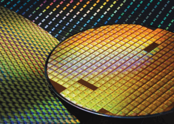
The U.S. Department of Commerce has awarded TSMC Arizona up to $6.6 billion in direct funding under the CHIPS Incentives Program to bolster domestic semiconductor production. The funding will support TSMC’s $65 billion investment in three advanced semiconductor fabrication facilities in Phoenix, Arizona. These fabs are designed to produce cutting-edge chips for applications such as artificial intelligence, 5G/6G networks, autonomous vehicles, and high-performance computing. The funds will be released incrementally as TSMC meets key milestones related to construction, production, and commercialization.

This initiative is part of a larger national effort to reduce reliance on foreign semiconductor production and strengthen U.S. technological and economic security. At full capacity, the Phoenix fabs are projected to produce millions of high-performance chips annually, including A16 semiconductors, the most advanced technology in TSMC’s portfolio. The project is expected to create approximately 6,000 direct manufacturing jobs and over 20,000 unique construction jobs. It marks the largest foreign direct investment in a greenfield project in U.S. history and highlights the Department of Commerce’s commitment to reshoring critical technologies.

TSMC Arizona will also benefit from up to $5 billion in proposed loans, authorized under the CHIPS and Science Act. These loans will complement direct funding to accelerate the development of the facilities. Early production at TSMC’s first Arizona fab, set to fully open next year, has already achieved yields comparable to similar facilities in Taiwan. The CHIPS Program Office will monitor the performance of the award through regular financial and programmatic reporting.

• Key Points:

• TSMC Arizona received up to $6.6 billion in CHIPS funding and $5 billion in proposed loans.

• The investment supports three state-of-the-art fabs in Phoenix, Arizona, with a total budget exceeding $65 billion.

• The facilities will produce advanced chips for AI, 5G/6G, autonomous vehicles, and other applications.

• Approximately 6,000 manufacturing jobs and 20,000 construction jobs are anticipated.

• The first fab is on track to open fully next year, producing leading-edge A16 semiconductors.

“Entering this phase of the U.S. CHIPS and Science Act marks a pivotal step in strengthening the semiconductor ecosystem in the United States,” said TSMC Chairman and CEO Dr. C.C. Wei. “This agreement helps us accelerate the development of the most advanced semiconductor manufacturing technology available in the U.S.”

Tags: CHIPs ActTSMC
ShareTweetShare
Previous Post

SoftBank Unveils AITRAS: Converged AI-RAN based on NVIDIA Aerial

Next Post

European Photonic Chip Pilot Plant to be Built in the Netherlands

Jim Carroll

Jim Carroll

Editor and Publisher, Converge! Network Digest, Optical Networks Daily - Covering the full stack of network convergence from Silicon Valley

Related Posts

Alphawave Semi Tapes Out UCIe 3D Chiplet on TSMC
Semiconductors

Alphawave Semi Tapes Out UCIe 3D Chiplet on TSMC

October 1, 2025
Alchip and Ayar Labs Team on Co-Packaged Optics
All

Alchip and Ayar Labs Team on Co-Packaged Optics

September 26, 2025
NIST Issues Broad Agency Announcement to Advance U.S. Microelectronics
Semiconductors

NIST Issues Broad Agency Announcement to Advance U.S. Microelectronics

September 25, 2025
Cadence Expands TSMC Partnership with AI-Driven Design
Semiconductors

Cadence Expands TSMC Partnership with AI-Driven Design

September 25, 2025
Polar Semi lands funding to become US-owned merchant fab
Semiconductors

Alphawave Semi Tapes Out 64 Gbps UCIe Gen3 on TSMC 3nm

September 24, 2025
Intel expands its manufacturing plans
Semiconductors

TSMC and University of Tokyo Launch Joint Semiconductor Lab

June 11, 2025
Next Post
Corning Introduces a New Material for EUV Chipmaking

European Photonic Chip Pilot Plant to be Built in the Netherlands

Categories

  • 5G / 6G / Wi-Fi
  • AI Infrastructure
  • All
  • Automotive Networking
  • Blueprints
  • Clouds and Carriers
  • Data Centers
  • Enterprise
  • Explainer
  • Feature
  • Financials
  • Last Mile / Middle Mile
  • Legal / Regulatory
  • Optical
  • Quantum
  • Research
  • Security
  • Semiconductors
  • Space
  • Start-ups
  • Subsea
  • Sustainability
  • Video
  • Webinars

Archives

Tags

5G All AT&T Australia AWS Blueprint columns BroadbandWireless Broadcom China Ciena Cisco Data Centers Dell'Oro Ericsson FCC Financial Financials Huawei Infinera Intel Japan Juniper Last Mile Last Mille LTE Mergers and Acquisitions Mobile NFV Nokia Optical Packet Systems PacketVoice People Regulatory Satellite SDN Service Providers Silicon Silicon Valley StandardsWatch Storage TTP UK Verizon Wi-Fi
Converge Digest

A private dossier for networking and telecoms

Follow Us

  • Home
  • Events Calendar
  • Blueprint Guidelines
  • Privacy Policy
  • Subscribe to Daily Newsletter
  • NextGenInfra.io

© 2025 Converge Digest - A private dossier for networking and telecoms.

No Result
View All Result
  • Home
  • Events Calendar
  • Blueprint Guidelines
  • Privacy Policy
  • Subscribe to Daily Newsletter
  • NextGenInfra.io

© 2025 Converge Digest - A private dossier for networking and telecoms.

This website uses cookies. By continuing to use this website you are giving consent to cookies being used. Visit our Privacy and Cookie Policy.
Go to mobile version