• Home
  • Events Calendar
  • Blueprint Guidelines
  • Privacy Policy
  • Subscribe to Daily Newsletter
  • NextGenInfra.io
No Result
View All Result
Converge Digest
Saturday, April 18, 2026
  • Home
  • Events Calendar
  • Blueprint Guidelines
  • Privacy Policy
  • Subscribe to Daily Newsletter
  • NextGenInfra.io
No Result
View All Result
Converge Digest
No Result
View All Result

Home » U.S. advances plan for national semiconductor research facilities

U.S. advances plan for national semiconductor research facilities

July 16, 2024
in All, Semiconductors
A A

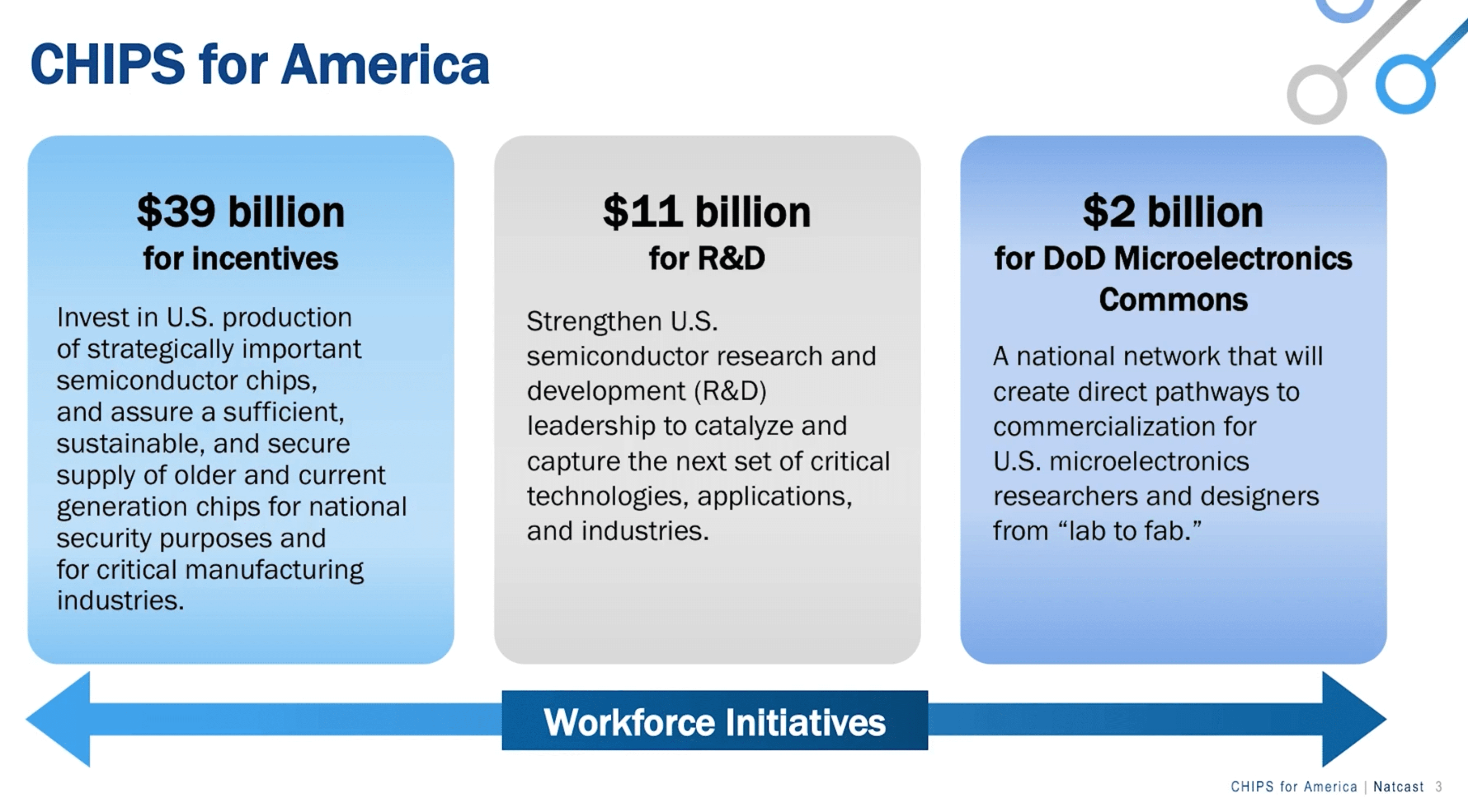
The Department of Commerce and Natcast, operator of the National Semiconductor Technology Center (NSTC), have initiated the selection process for the first three R&D facilities funded by the CHIPS and Science Act. These facilities are integral to President Biden’s Investing in America agenda, which aims to bolster the U.S. semiconductor ecosystem through advanced R&D and job creation.

The Three Facilities:

1. NSTC Prototyping and NAPMP Advanced Packaging Piloting Facility: This state-of-the-art center will combine next-generation manufacturing and packaging technologies, providing 300mm research, prototyping, and packaging capabilities. It will co-locate NSTC R&D and NAPMP packaging capabilities to facilitate collaborative semiconductor and advanced packaging research.

2. NSTC Administrative and Design Facility: A multi-functional center housing key NSTC operations, including administrative functions, consortium member meetings, and programmatic activities like the Workforce Center of Excellence and the NSTC Design Enablement Gateway. It will focus on advanced semiconductor research in chip design, electronic design automation, chip and system architecture, and hardware security.

3. NSTC EUV Center: This facility will provide access to EUV lithography technology, essential for cutting-edge semiconductor research and commercialization. It will also offer space for Natcast researchers, staff, and member assignees to collaborate on advanced projects.

The selection process for these facilities started today, with the Department and Natcast planning to release additional information on affiliated technical centers soon. Expected operational dates are 2025 for the NSTC Administrative and Design Facility, 2026 for the NSTC EUV Center, and 2028 for the NSTC Prototyping and NAPMP Advanced Packaging Piloting Facility.

These facilities will drive innovation, create differentiation, ensure financial sustainability, and foster thriving ecosystems. They will bridge the gap between research and industry, securing the U.S.’s leadership in semiconductor manufacturing and research for decades to come.

For more details, visit Natcast’s website and view their informational video.

Source: NIST
Tags: CHIPs Act
ShareTweetShare
Previous Post

BT: Record traffic as 11.5 Million UK homes stream Euro 2024

Next Post

Juniper opens Ops4AI Lab in Silicon Valley

Jim Carroll

Jim Carroll

Editor and Publisher, Converge! Network Digest, Optical Networks Daily - Covering the full stack of network convergence from Silicon Valley

Related Posts

NIST Issues Broad Agency Announcement to Advance U.S. Microelectronics
Semiconductors

NIST Issues Broad Agency Announcement to Advance U.S. Microelectronics

September 25, 2025
Natcast Leads U.S. National Semiconductor Technology Center with $6.3B Funding
Semiconductors

Natcast Leads U.S. National Semiconductor Technology Center with $6.3B Funding

January 16, 2025
U.S. advances plan for national semiconductor research facilities
Semiconductors

U.S. Department of Commerce Allocates $1.4 Billion for Advanced Semiconductor Packaging

January 16, 2025
CHIPS for America allocates $3 billion for National Advanced Packaging
Semiconductors

Four More Companies Land $264M in CHIPs Act Funding

January 16, 2025
MACOM posts revenue of $178.1 million, up 14.8% yoy
Semiconductors

MACOM Unveils $345M Plan to Modernize Semiconductor Facilities

January 14, 2025
U.S. advances plan for national semiconductor research facilities
All

Amkor Secures $407M CHIPS Grant for Advanced Packaging

December 26, 2024
Next Post
Silicon Valley Bets Big on Campus Network-as-a-Service

Silicon Valley Bets Big on Campus Network-as-a-Service

Categories

  • 5G / 6G / Wi-Fi
  • AI Infrastructure
  • All
  • Automotive Networking
  • Blueprints
  • Clouds and Carriers
  • Data Centers
  • Enterprise
  • Explainer
  • Feature
  • Financials
  • Last Mile / Middle Mile
  • Legal / Regulatory
  • Optical
  • Quantum
  • Research
  • Security
  • Semiconductors
  • Space
  • Start-ups
  • Subsea
  • Sustainability
  • Video
  • Webinars

Archives

Tags

5G All AT&T Australia AWS Blueprint columns BroadbandWireless Broadcom China Ciena Cisco Data Centers Dell'Oro Ericsson FCC Financial Financials Huawei Infinera Intel Japan Juniper Last Mile Last Mille LTE Mergers and Acquisitions Mobile NFV Nokia Optical Packet Systems PacketVoice People Regulatory Satellite SDN Service Providers Silicon Silicon Valley StandardsWatch Storage TTP UK Verizon Wi-Fi
Converge Digest

A private dossier for networking and telecoms

Follow Us

  • Home
  • Events Calendar
  • Blueprint Guidelines
  • Privacy Policy
  • Subscribe to Daily Newsletter
  • NextGenInfra.io

© 2025 Converge Digest - A private dossier for networking and telecoms.

No Result
View All Result
  • Home
  • Events Calendar
  • Blueprint Guidelines
  • Privacy Policy
  • Subscribe to Daily Newsletter
  • NextGenInfra.io

© 2025 Converge Digest - A private dossier for networking and telecoms.

This website uses cookies. By continuing to use this website you are giving consent to cookies being used. Visit our Privacy and Cookie Policy.
Go to mobile version