At the Hot Chips Conference at Stanford University, Darius Bunandar, Chief Scientist and Founder of Lightmatter, previewed his presentation on the company’s groundbreaking Passage M1000 3D photonic interposer for AI workloads.
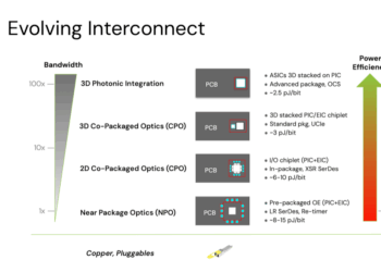
Lightmatter is pioneering the integration of silicon photonics into advanced compute systems, with the goal of overcoming the “shoreline limitation” in chip design—where communication bandwidth is restricted by the perimeter of a chip. By introducing a 3D photonic interposer, Lightmatter places optical engines directly beneath the compute die, unlocking the ability to move data across the entire surface area rather than just the edges.
In this clip, Darius explains why this approach is so revolutionary for scaling AI systems. He describes how the M1000 reference design integrates a multi-tile photonic IC with 34 chiplets in a chip-on-wafer process, delivering 1,024 SerDes lanes inside a single package. This unprecedented bandwidth density could transform the way future AI clusters are built.

Timestamps:
00:00 – Why shoreline-limited interconnects constrain scaling
00:18 – How 3D photonic packaging changes the paradigm
00:47 – The exponential gap between compute and interconnect
01:06 – Industry partnerships with GlobalFoundries and Amkor
01:20 – Inside the Passage M1000: 34 chiplets, multi-tile photonics, and 1,024 SerDes
01:47 – Unprecedented bandwidth density in a single package
Have a tech update that you want to brief us on? Contact info@nextgeninfra.io!