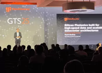
Silicon photonics has reached a critical inflection point as AI and generative workloads drive unprecedented demand for bandwidth, power efficiency, and scalable interconnects. In this interview, Vikas Gupta, Senior Director of Product Management at GlobalFoundries, explains how GF is enabling 200G and 400G per wavelength solutions, advancing microring resonator technology, and building end-to-end packaging capabilities at its Malta, NY facility.
From scale-out data center networking to scale-up GPU and AI accelerator interconnects, GF is positioning its silicon photonics platform to support the exponential growth of generative AI. Gupta highlights GF’s leadership in microring modulators, multi-lambda DWDM circuits, and the advanced manufacturing innovations required to produce these devices in high volume across 300mm wafers. He also details the company’s significant CapEx investments in photonics and packaging, including its new Firebird advanced photonics and packaging center.

Timestamps:
00:00 – Silicon photonics reaches an inflection point with AI demand
00:30 – Transition from 100G to 200G and 400G per wavelength
00:44 – Two types of networks: scale-out vs. scale-up in AI data centers
01:10 – GF’s leadership in microring modulators and DWDM
01:36 – Manufacturing challenges: heater control, variability, and 300mm wafer scale
02:07 – GF investments in Malta fab and Firebird photonics & packaging center
02:40 – Advanced packaging: bumping, TSV stacking, detachable fiber attach
02:53 – Why GF is doubling down on silicon photonics now
Have a tech update that you want to brief us on? Contact info@nextgeninfra.io!
Check out other Tech Updates on our YouTube Channel (subscribe today): https://www.youtube.com/@NextGenInfra and check out our latest reports at: https://nextgeninfra.io/