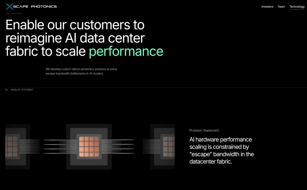
Xscape Photonics and Tower Semiconductor introduced an on-chip, optically pumped, multi-wavelength laser platform designed for AI datacenter fabrics. The prototype, available as a validation kit, is built on Tower’s PH18 silicon photonics platform and enables coarse and dense wavelength division multiplexing (CWDM/DWDM) optical fabrics. By embedding programmable, multi-color lasers directly on-chip and powering them with a single external continuous-wave (CW) laser, the solution removes the need for multiple discrete laser sources or hybrid III-V integration.
The platform, called ChromX, leverages Xscape’s proprietary CombX programmable laser source technology. It provides a scalable upgrade path for AI fabrics that require high bandwidth density, low power consumption, and reduced latency. Fully compatible with existing PH18 photonic components such as modulators and detectors, the on-chip laser approach simplifies packaging, cuts component count, and strengthens reliability for GPU-to-GPU and GPU-to-HBM optical links in large AI clusters. Backed by investors including NVIDIA and Cisco, Xscape Photonics positions itself at the intersection of optical interconnect innovation and AI infrastructure demand.
- Industry-first monolithic, optically pumped on-chip multi-wavelength laser
- Built on Tower’s PH18 silicon photonics platform, validated and shipping in prototype kits
- Compatible with CWDM/DWDM grids for scalable AI datacenter fabrics
- Eliminates hybrid III-V integration and reduces packaging complexity
- Backed by NVIDIA and Cisco; targeted for GPU and memory interconnects in disaggregated AI clusters
“Our close collaboration with Tower has allowed us to bring to market a highly differentiated, manufacturable, and scalable solution,” said Vivek Raghunathan, CEO of Xscape Photonics. “By building on Tower’s proven and qualified high-volume PH18 platform, we’ve eliminated the need for costly hybrid laser integration and delivered the first monolithically integrated, multi-color laser source directly on-chip. This will transform how AI fabrics are architected going forward.”
🌐 Analysis: Xscape Photonics is tackling one of the hardest problems in silicon photonics—integrating lasers directly onto CMOS-compatible wafers without III-V hybridization. Its CombX technology and ChromX platform offer programmability and multi-color operation, critical for CWDM/DWDM scaling in AI fabrics. Tower Semiconductor provides the foundry muscle, with its PH18 process already qualified for high-volume photonics. Competitors such as Ayar Labs and Ranovus have focused on CPO and laser integration via hybrid methods, but Xscape’s approach could reshape optical interconnect economics by reducing supply chain complexity. With NVIDIA and Cisco backing, the company is well-positioned in a market set to double in size by mid-decade.
Xscape Photonics is a Santa Clara, California–based startup (with an additional office in Fort Lee, NJ) developing advanced silicon photonics platforms for AI data center interconnects . Founded in 2022 by leading Columbia researchers Keren Bergman, Michal Lipson, Alexander Gaeta, and Yoshi Okawachi, alongside CEO Vivek Raghunathan, the team brings deep expertise in silicon photonics, laser engineering, and scalable compute infrastructure. The company’s mission is to tackle the “escape bandwidth” bottlenecks in AI clusters by dramatically improving bandwidth, power efficiency, and scalability via its proprietary ChromX multi‑color photonics platform—capable of scaling from tens to hundreds of wavelengths per optical fiber, delivering up to ~10× improvements in bandwidth and energy efficiency .
The firm raised a $44 million Series A in October 2024—led by IAG Capital Partners with participation from Altair, Cisco Investments, NVIDIA, Fathom Fund, Kyra Ventures, LifeX Ventures, and OUP—bringing total funding to about $57 million
🌐 We’re tracking the latest developments in networking silicon. Follow our ongoing coverage at: https://convergedigest.com/category/semiconductors/