• Home
  • Events Calendar
  • Blueprint Guidelines
  • Privacy Policy
  • Subscribe to Daily Newsletter
  • NextGenInfra.io
No Result
View All Result
Converge Digest
Saturday, April 18, 2026
  • Home
  • Events Calendar
  • Blueprint Guidelines
  • Privacy Policy
  • Subscribe to Daily Newsletter
  • NextGenInfra.io
No Result
View All Result
Converge Digest
No Result
View All Result

Home » IBM Builds Carbon Nanotube Chip

IBM Builds Carbon Nanotube Chip

October 28, 2012
in All
A A

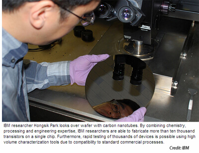
IBM announced a breakthrough in building a semiconductor using carbon nanotubes instead of silicon.  IBM researchers created a device consisting of more than ten thousand working transistors made of nano-sized tubes of carbon.  Standard semiconductor processes were used to fabricate the device.


IBM has previously demonstrated that carbon nanotube transistors can operate as excellent switches at molecular dimensions of less than ten nanometers – less than half the size of the leading silicon technology. 


“Carbon nanotubes, borne out of chemistry, have largely been laboratory curiosities as far as microelectronic applications are concerned. We are attempting the first steps towards a technology by fabricating carbon nanotube transistors within a conventional wafer fabrication infrastructure,” said Supratik Guha, Director of Physical Sciences at IBM Research. “The motivation to work on carbon nanotube transistors is that at extremely small nanoscale dimensions, they outperform transistors made from any other material. However, there are challenges to address such as ultra high purity of the carbon nanotubes and deliberate placement at the nanoscale. We have been making significant strides in both.” 


http://www-03.ibm.com/press/us/en/pressrelease/39250.wss

In November 2010, IBM announced significant advances in its path to integrate electrical and optical devices on the same piece of silicon. The new CMOS Integrated Silicon Nanophotonics, which is the result of a decade of development at IBM’s global Research laboratories, promises over 10X improvement in integration density than is feasible with current manufacturing techniques.


At the time, IBM said it anticipates that Silicon Nanophotonics will dramatically increase the speed and performance between chips. In addition to combining electrical and optical devices on a single chip, the new IBM technology can be produced on the front-end of a standard CMOS manufacturing line. Transistors can share the same silicon layer with silicon nanophotonics devices. To make this approach possible, IBM researchers have developed a suite of integrated ultra-compact active and passive silicon nanophotonics devices that are all scaled down to the diffraction limit — the smallest size that dielectric optics can afford. This makes possible the integration of modulators, germanium photodetectors and ultra-compact wavelength-division multiplexers with high-performance analog and digital CMOS circuitry. 

“The development of the Silicon Nanophotonics technology brings the vision of on-chip optical interconnections much closer to reality,” said Dr. T.C. Chen, vice president, Science and Technology, IBM Research. “With optical communications embedded into the processor chips, the prospect of building power-efficient computer systems with performance at the Exaflop level is one step closer to reality.”

  • In March 2010, IBM announced a Germanium Avalanche Photodetector working at 40 Gbps with CMOS compatible voltages as low as 1.5V. This was the last piece of the puzzle that completes the prior development of the “nanophotonics toolbox of devices necessary to build the on-chip interconnects.

  • In March 2008, IBM scientists announced the world’s tiniest nanophotonic switch for “directing traffic” in on-chip optical communications, ensuring that optical messages can be efficiently routed.

  • In December 2007, IBM scientists announced the development of an ultra-compact silicon electro-optic modulator, which converts electrical signals into the light pulses, a prerequisite for enabling on-chip optical communications.

  • In December 2006, IBM scientists demonstrated silicon nanophotonic delay line that was used to buffer over a byte of information encoded in optical pulses – a requirement for building optical buffers for on-chip optical communications.
  • http://www.research.ibm.com/photonics

    Tags: Blueprint columnsSilicon Photonics
    ShareTweetShare
    Previous Post

    América Móvil Hits 319 Million Accesses

    Next Post

    Xilinx Announces Defense-Grade 7 Series FPGAs

    Staff

    Staff

    Related Posts

    DustPhotonics Debuts 1.6T and 800G 2xFR4 Chips
    All

    DustPhotonics Debuts 1.6T and 800G 2xFR4 Chips

    April 2, 2025
    Openlight samples its 2x FR4 Photonic ASIC
    Optical

    OpenLight Partners with DoplayDo to Streamline Silicon Photonics Design

    January 28, 2025
    Silicon Photonics Industry Alliance Gets Underway, Backed by TSMC
    Optical

    Silicon Photonics Industry Alliance Gets Underway, Backed by TSMC

    September 4, 2024
    Intel highlights 4 Tbps optical compute interconnect chiplet
    All

    Intel highlights 4 Tbps optical compute interconnect chiplet

    June 26, 2024
    Blueprint: Brazil looks to municipal Wi-Fi 6E
    Blueprints

    Blueprint: Brazil looks to municipal Wi-Fi 6E

    February 21, 2023
    OpenLight appoints Adam Carter as CEO
    Optical

    OpenLight appoints Adam Carter as CEO

    January 18, 2023
    Next Post
    Xilinx Announces Defense-Grade 7 Series FPGAs

    Xilinx Announces Defense-Grade 7 Series FPGAs

    Please login to join discussion

    Categories

    • 5G / 6G / Wi-Fi
    • AI Infrastructure
    • All
    • Automotive Networking
    • Blueprints
    • Clouds and Carriers
    • Data Centers
    • Enterprise
    • Explainer
    • Feature
    • Financials
    • Last Mile / Middle Mile
    • Legal / Regulatory
    • Optical
    • Quantum
    • Research
    • Security
    • Semiconductors
    • Space
    • Start-ups
    • Subsea
    • Sustainability
    • Video
    • Webinars

    Archives

    Tags

    5G All AT&T Australia AWS Blueprint columns BroadbandWireless Broadcom China Ciena Cisco Data Centers Dell'Oro Ericsson FCC Financial Financials Huawei Infinera Intel Japan Juniper Last Mile Last Mille LTE Mergers and Acquisitions Mobile NFV Nokia Optical Packet Systems PacketVoice People Regulatory Satellite SDN Service Providers Silicon Silicon Valley StandardsWatch Storage TTP UK Verizon Wi-Fi
    Converge Digest

    A private dossier for networking and telecoms

    Follow Us

    • Home
    • Events Calendar
    • Blueprint Guidelines
    • Privacy Policy
    • Subscribe to Daily Newsletter
    • NextGenInfra.io

    © 2025 Converge Digest - A private dossier for networking and telecoms.

    No Result
    View All Result
    • Home
    • Events Calendar
    • Blueprint Guidelines
    • Privacy Policy
    • Subscribe to Daily Newsletter
    • NextGenInfra.io

    © 2025 Converge Digest - A private dossier for networking and telecoms.

    This website uses cookies. By continuing to use this website you are giving consent to cookies being used. Visit our Privacy and Cookie Policy.
    Go to mobile version