• Home
  • Events Calendar
  • Blueprint Guidelines
  • Privacy Policy
  • Subscribe to Daily Newsletter
  • NextGenInfra.io
No Result
View All Result
Converge Digest
Friday, April 17, 2026
  • Home
  • Events Calendar
  • Blueprint Guidelines
  • Privacy Policy
  • Subscribe to Daily Newsletter
  • NextGenInfra.io
No Result
View All Result
Converge Digest
No Result
View All Result

Home » IBM Develops Ultra-Fast Analog-to-Digital Converter

IBM Develops Ultra-Fast Analog-to-Digital Converter

February 13, 2014
in All
A A

IBM Research and Ecole Polytechnique Fédérale de Lausanne (EPFL) have developed an ultra-fast and energy efficient analog-to-digital converter (ADC) technology to enable complex digital equalization across long-distance fiber channels.

An ADC converts analog signals to digital, approximating the right combination of zeros and ones to digitally represent the data so it can be stored on computers and analyzed for patterns and predictive outcomes.

IBM has awarded a non-exclusive technology license to Semtech, including access to patented designs and technological know-how, to develop the technology for its own family of products ranging from optical and wireline communications to advanced radar systems.

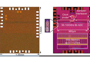
The 64 GS/s (giga-samples per second) chips for Semtech will be manufactured at IBM’s 300mm fab in East Fishkill, New York in a 32 nanometer silicon-on-insulator CMOS process and has an area of 5 mm2. This core includes a wide tuning millimeter wave synthesizer enabling the core to tune from 42 to 68 GS/s per channel with a nominal jitter value of 45 femtoseconds root mean square. The full dual-channel 2×64 GS/s ADC core generates 128 billion analog-to-digital conversions per second, with a total power consumption of 2.1 Watts.

IBM cited a number of Big Data use cases, including radio astronomy projects that are expected to produce 10 times the global internet traffic loads in a few years.

“Our ADC supports IEEE standards for data communication and brings together speed and energy efficiency at 32 nanometers enabling us to start tackling the largest Big Data applications,” said Dr. Martin Schmatz, Systems department manager at IBM Research. “With Semtech as our partner, we are bringing our previous generation of the ADC to market less than 12 months since it was first developed and tested.”

“Through leveraging the IBM 32nm SOI process with its unique feature set, we are developing products that are well-suited for meeting the challenge presented by the next step in high performance  communications systems such as 400 Gb/s Optical systems and Advanced Radar systems. We are also seeing an expanding range of applications in the existing radio frequency communications marketplace where high-speed digital logic is replacing functions that have been traditionally performed by less flexible analog circuitry,” said Craig Hornbuckle, Chief Systems Architect, Semtech.

http://www-03.ibm.com/press/us/en/pressrelease/43171.wss

Tags: 400GBlueprint columnsIBMSilicon
ShareTweetShare
Previous Post

Gigamon Partners with Vistapointe on Big Data Monitoring + Network Intelligence

Next Post

NTT and Partners Demo NFV Service Chaining

Staff

Staff

Related Posts

IBM and Cisco Aim for Networked, Fault-Tolerant Quantum by Early 2030s
Quantum

IBM and Cisco Aim for Networked, Fault-Tolerant Quantum by Early 2030s

November 20, 2025
IBM Doubles Quantum R&D Speed With 300 mm Fab
Quantum

IBM Doubles Quantum R&D Speed With 300 mm Fab

November 12, 2025
Airtel and IBM Partner to Expand AI-Ready Cloud Infrastructure
All

Airtel and IBM Partner to Expand AI-Ready Cloud Infrastructure

October 23, 2025
IBM Launches Spyre Accelerator to Power Generative and AgenticAI
Data Centers

IBM Launches Spyre Accelerator to Power Generative and AgenticAI

October 8, 2025
Video: AI Automation for Real-Time, Multi-Vendor Networks
Video

#AINetworking25: What’s Next for AI-Driven Networking – Director’s Cut

October 6, 2025
IBM Launches Power11 Server Family with AI Acceleration
Data Centers

IBM Launches Power11 Server Family with AI Acceleration

July 8, 2025
Next Post
NTT and Partners Demo NFV Service Chaining

NTT and Partners Demo NFV Service Chaining

Please login to join discussion

Categories

  • 5G / 6G / Wi-Fi
  • AI Infrastructure
  • All
  • Automotive Networking
  • Blueprints
  • Clouds and Carriers
  • Data Centers
  • Enterprise
  • Explainer
  • Feature
  • Financials
  • Last Mile / Middle Mile
  • Legal / Regulatory
  • Optical
  • Quantum
  • Research
  • Security
  • Semiconductors
  • Space
  • Start-ups
  • Subsea
  • Sustainability
  • Video
  • Webinars

Archives

Tags

5G All AT&T Australia AWS Blueprint columns BroadbandWireless Broadcom China Ciena Cisco Data Centers Dell'Oro Ericsson FCC Financial Financials Huawei Infinera Intel Japan Juniper Last Mile Last Mille LTE Mergers and Acquisitions Mobile NFV Nokia Optical Packet Systems PacketVoice People Regulatory Satellite SDN Service Providers Silicon Silicon Valley StandardsWatch Storage TTP UK Verizon Wi-Fi
Converge Digest

A private dossier for networking and telecoms

Follow Us

  • Home
  • Events Calendar
  • Blueprint Guidelines
  • Privacy Policy
  • Subscribe to Daily Newsletter
  • NextGenInfra.io

© 2025 Converge Digest - A private dossier for networking and telecoms.

No Result
View All Result
  • Home
  • Events Calendar
  • Blueprint Guidelines
  • Privacy Policy
  • Subscribe to Daily Newsletter
  • NextGenInfra.io

© 2025 Converge Digest - A private dossier for networking and telecoms.

This website uses cookies. By continuing to use this website you are giving consent to cookies being used. Visit our Privacy and Cookie Policy.
Go to mobile version